Technique for doping compound layers used in solar cell fabrication

a technology of solar cells and compound layers, which is applied in the direction of electrical equipment, basic electric elements, semiconductor devices, etc., can solve the problems of low material non-uniformity of cigs layers, and high equipment cost, so as to achieve low materials utilization and high equipment cost

Inactive Publication Date: 2008-01-31
SOLOPOWER
View PDF10 Cites 38 Cited by
  • Summary
  • Abstract
  • Description
  • Claims
  • Application Information

AI Technical Summary

Benefits of technology

[0006] The first technique that yielded high-quality Cu(In,Ga)Se2 films for solar cell fabrication was co-evaporation of Cu, In, Ga and Se onto a heated substrate in a vacuum chamber. This is an approach with low materials utilization and high cost of equipment.
[0007] Another technique for growing Cu(In,Ga)(S,Se)2 type compound thin films for solar cell applications is a two-stage process where metallic components of the Cu(In,Ga)(S,Se)2 material are first deposited onto a substrate, and then reacted with S and / or Se in a high temperature annealing process. For example, for CuInSe2 growth, thin layers of Cu and In are first deposited on a substrate and then this stacked precursor layer is reacted with Se at elevated temperature. If the reaction atmosphere also contains sulfur, then a CuIn(S,Se)2 layer can be grown. Addition of Ga in the precursor layer, i.e. use of a Cu / In / Ga stacked film precursor, allows the growth of a Cu(In,Ga)(S,Se)2 absorber.

Problems solved by technology

However, the cost of electricity generated using silicon-based solar cells is higher than the cost of electricity generated by the more traditional methods.
This is an approach with low materials utilization and high cost of equipment.
This is, however, an uncontrolled process and causes non-uniformities in the CIGS layers depending on how much Na diffuses from the substrate through the Mo contact layer.
In wet coating approaches such as electroless plating and electroplating this may not be possible.
Since such wet techniques are surface sensitive and may be carried out of aqueous solutions nucleation on materials such as NaF and NaCl may not be good or even possible.
Therefore, a precursor layer such as a Cu / In / Ga stack or a precursor layer comprising Cu, In, Ga and optionally Se may not be electrodeposited in a reliable and repeatable manner on substrates comprising a Na source on their surface.
Furthermore, PVD techniques typically used to deposit Na-containing interfacial layers are expensive methods that increase cost of production.
As the review above demonstrates, controlled doping of Group IBIIIAVIA compound layers with alkali metals improve their quality in terms of yielding higher efficiency solar cell devices, however, low cost approaches are needed to include such dopants into the growing film in a controlled manner.

Method used


Image

  • Technique for doping compound layers used in solar cell fabrication
  • Technique for doping compound layers used in solar cell fabrication

Examples


Embodiment Construction

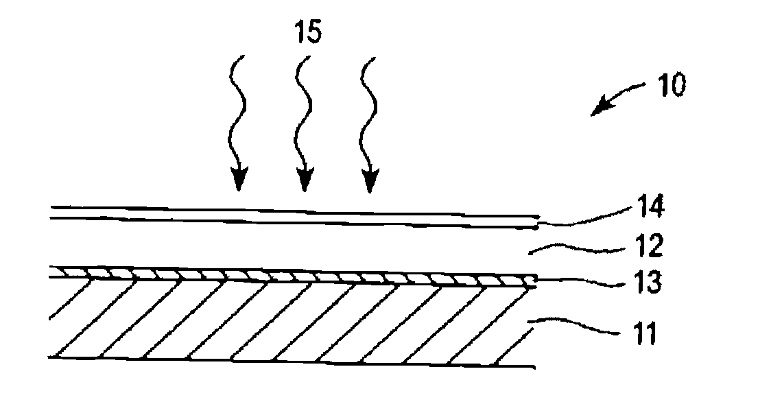
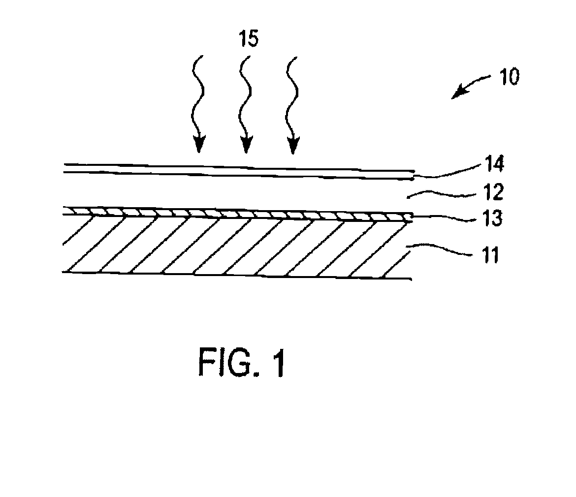
[0018] There are various ways of growing Group IBIIIAVIA compound films such as Cu(In,Ga)(S,Se)2 compound layers utilizing wet techniques such as electrodeposition. In one approach all the group IB and Group IIIA elements of the compound, i.e. Cu, In and Ga are electroplated on a base in the form of discrete layers forming a stacked precursor layer with a structure such as Cu / Ga / In, or Cu / In / Ga, or Cu / Ga / Cu / In, or Cu / In / Cu / Ga, etc. This precursor layer is then reacted with at least one of S and Se to form the Cu(In,Ga)(Se,S)2 compound layer. It is also possible to use a hybrid approach where only some of the constituents of the compound are electrodeposited. For example, one can deposit Cu by PVD and Ga and In by electrodeposition to form a precursor layer comprising Cu, In and Ga and then react this precursor layer with at least one of Se and S to form the compound. The present invention achieves controlled doping of the compound layer by including at least one alkali metal in the ...


PUM

PropertyMeasurementUnit
molar ratioaaaaaaaaaa
temperatureaaaaaaaaaa
concentrationaaaaaaaaaa

Abstract

The present invention includes methods and apparatus therefrom for preparing thin films of doped semiconductors for radiation detector and photovoltaic applications, and particularly method and apparatus that increase dopants of alkali metals in Group IBIIIAVIA layers. In a particular aspect, the present invention includes a method of preparing a doped Group IBIIIAVIA absorber layer for a solar cell, with the absorber layer being formed by reaction, with a Group VIA material, of a metallic stack with a plurality of layers, in which each layer contains a concentration of an alkali metal selected from the group of Na, K and Li.

Description

CLAIM OF PRIORITY [0001] This application claims priority to and incorporates herein by reference U.S. Provisional Appln. Ser. No. 60 / 820,479 filed Jul. 26, 2006 entitled “Technique for Doping Compound Layers Used in Solar Cell Fabrication; and is related to U.S. application Ser. No. 11 / 081,308 filed Mar. 15, 2005 entitled “Technique and Apparatus for Depositing Thin Layers of Semiconductors for Solar Cell Fabrication”; U.S. application Ser. No. 11 / 266,013 filed Nov. 2, 2005 entitled “Technique and Apparatus for Depositing Layers of Semiconductors for Solar Cell and Module Fabrication”; U.S. application Ser. No. 11 / 462,685 filed Aug. 4, 2006 entitled “Technique for Preparing Precursor Films and Compound Layers For Thin Film Solar Cell Fabrication”; and U.S. application Ser. No. 11 / 535,927 filed Sep. 27, 2006 entitled “Efficient Gallium Thin Film Electroplating Methods and Chemistries”.FIELD OF THE INVENTION [0002] The present invention relates to method and apparatus for preparing t...

Claims


Application Information

Patent Timeline
Patent Type & Authority Applications(United States)
IPC IPC(8): C25D5/10
CPCH01L31/0322Y02E10/541H01L31/0323
Inventor BASOL, BULENT M.
Owner SOLOPOWER
Why Eureka
Try Eureka