Method for fabricating charge-trapping memory

a charge-trapping memory and charge-trapping technology, applied in the field of charge-trapping memory fabrication, can solve the problems of large threshold voltage distribution, clustering of charges, and destruction of stored data, and achieve the effects of wide distribution of threshold voltage and serious consequences

Inactive Publication Date: 2008-01-31
MACRONIX INT CO LTD
View PDF14 Cites 0 Cited by
  • Summary
  • Abstract
  • Description
  • Claims
  • Application Information

AI Technical Summary

Benefits of technology

[0018]Since the wide threshold voltage distribution induced by plasma or UV light can be narrowed according to fabrication method of the present invention, data errors encountered in the charge-trapping memory device can be obviated. Moreover, the need for a protecting structure, such as fuse or diode, connecting to the metal line can be eliminated.

Problems solved by technology

If a defect occurs in the tunnel oxide film, the charges accumulated in the floating gate are likely to leak out, causing a destruction of the stored data.
However, the plasma used in the PECVD process often causes a clustering of charges on the surface of the insulating layer, wherein these charges travels to the silicon nitride layer in the ONO layer along the metal lines.
A wide distribution of the threshold voltage has serious consequences.
For example, if a memory has a wide threshold voltage distribution, the program distribution and erase distribution may overlap with each other, leading to an abnormal function of the memory device.

Method used


Image

  • Method for fabricating charge-trapping memory
  • Method for fabricating charge-trapping memory
  • Method for fabricating charge-trapping memory

Examples


Embodiment Construction

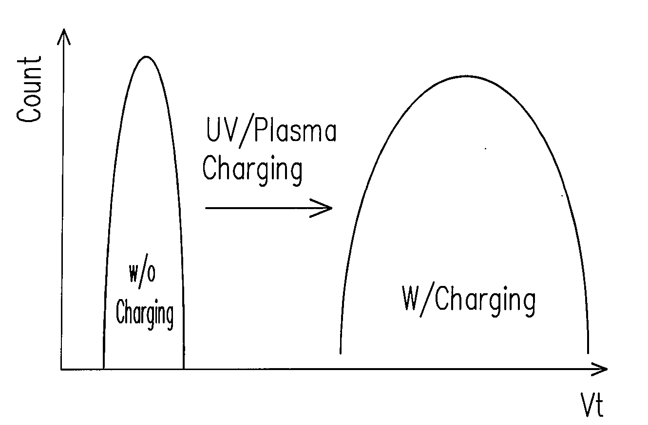
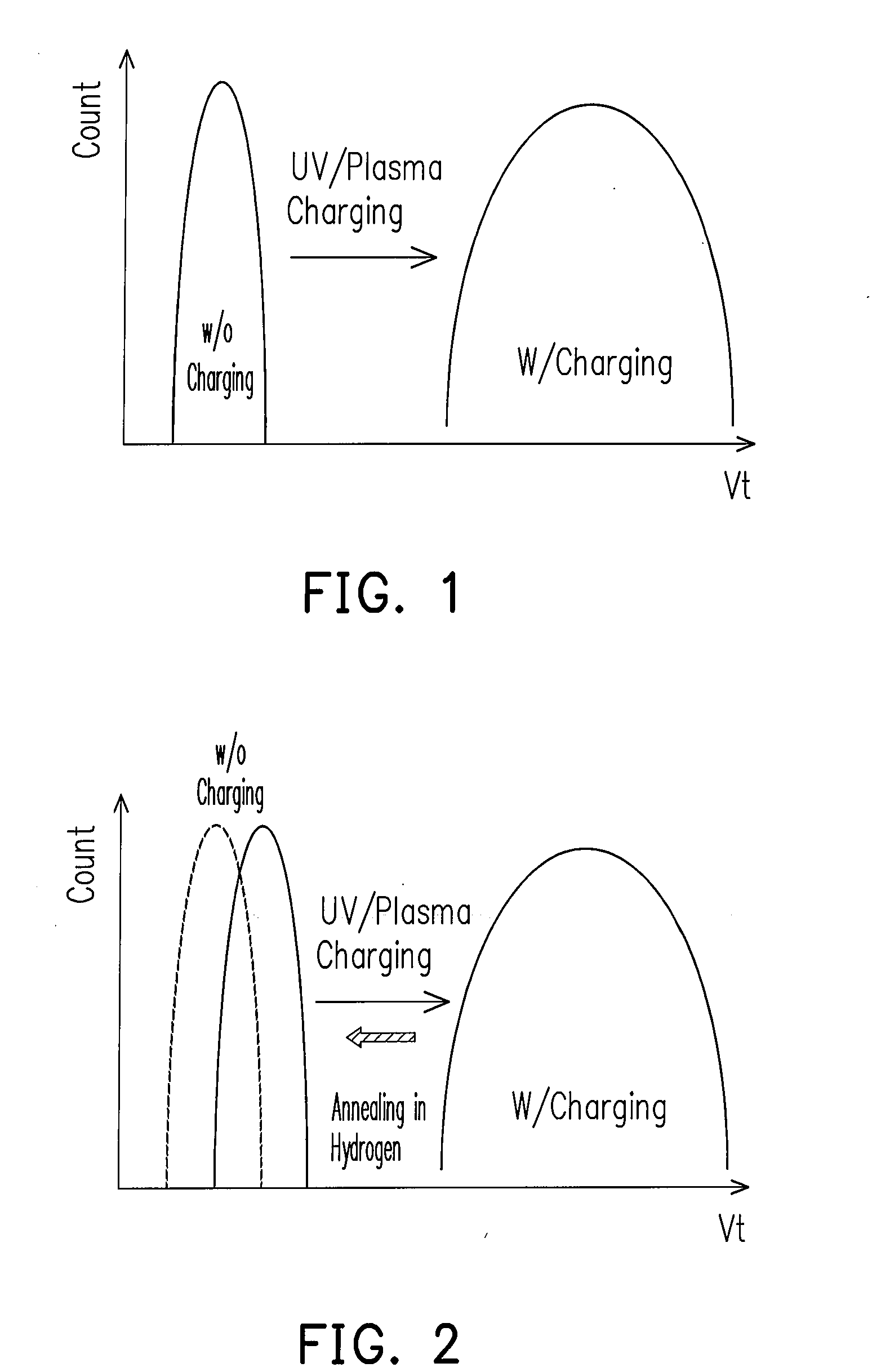
[0026]A wide threshold voltage distribution among devices may result due to unwanted electrons trapped in the charge-trapping medium. The charge-trapping medium with the unwanted electrons is charged by, for example plasma or ultraviolet light (UV) used in the device fabrication process. According to the method of the present invention for tightening a threshold voltage distribution of plasma or UV charged devices, an annealing process is conducted in hydrogen gas at about 350° C. to about 450° C. More preferably, the annealing process is conducted at about 400° C. Further, the annealing process may conduct with pure or diluted hydrogen gas. When the annealing process is conducted with diluted hydrogen gas, the hydrogen concentration is at least greater than 0.5 mole percent. More preferably, the hydrogen concentration is about 10 mole percent. As shown in FIG. 2, FIG. 2 is a schematic diagram illustrating the threshold voltage distributions among charged memory devices before versu...


PUM

PropertyMeasurementUnit
temperatureaaaaaaaaaa
threshold voltagesaaaaaaaaaa

Abstract

A manufacturing method of a charge-trapping memory device is provided. This method includes forming a stacked structure having at least a charge-trapping medium. An annealing process in a hydrogen gas is then performed on the stacked structure subsequent to the device fabrication process. The annealing process is conducted at a temperature of about 350° C. to 450° C. and with the concentration of the hydrogen gas greater than 0.5 mole percent.

Description

BACKGROUND OF THE INVENTION[0001]1. Field of Invention[0002]The present invention relates to a method for fabricating a semiconductor device. More particularly, the present invention relates to a method for fabricating a charge-trapping memory.[0003]2. Description of Related Art[0004]Flash memory is a type of non-volatile memory that allows multiple data reading, writing and erasing operations. In addition, the stored data are retained even after power to the device is terminated. With these advantages, flash memory has been broadly applied in personal computers and electronic equipment.[0005]A conventional flash memory is a device having a dual-gate structure, in which a first gate electrode that functions as a floating gate electrode is formed on an oxide film disposed on the surface of a semiconductor substrate, an interlayer insulating film is disposed on the upper surface of the first gate electrode, and a second gate electrode that functions as a control gate electrode is form...

Claims


Application Information

Patent Timeline
Patent Type & Authority Applications(United States)
IPC IPC(8): G11C16/04
CPCH01L21/76838H01L29/792H01L29/66833
Inventor SHIH, YEN-HAOHSIEH, JUNG-YUYANG, YI-LINCHANG, CHIA-HUAHWU, JENN-GWO
Owner MACRONIX INT CO LTD
Why Eureka
Try Eureka