
Flip-flop circuit

a flip-flop circuit and circuit technology, applied in the field of flip-flop circuits, can solve the problems of increasing the hold time, consuming unwanted power, and prolonging the delay time until the data is outputted, so as to reduce the power consumption, suppress unwanted operations, and reduce power consumption

Inactive Publication Date: 2008-02-07
SANYO ELECTRIC CO LTD
View PDF5 Cites 7 Cited by
  • Summary
  • Abstract
  • Description
  • Claims
  • Application Information

AI Technical Summary

Benefits of technology

[0015]The present invention has been made in view of the foregoing circumstances and a general purpose thereof is to provide a flip-flop circuit that operates with a reduced power consumption. An advantage of the present invention is to provide a flip-flop circuit with a short hold time.
[0016]One embodiment of the present invention relates to a flip-flop circuit. This flip-flop circuit includes a latch circuit which latches input data based on a first clock, wherein the latch circuit takes in the input data in a period of a phase difference between the first clock and a second clock whose phase differs from that of the first clock.
[0017]The “first clock” and the “second clock” may be in-phase with each other or in reverse phase with each other. In the case of in-phase, the input data may be taken in either in a period during which the first clock is high and the second clock is low or in a period during which the first clock is low and the second clock is high. In the case of reverse phase, the input data may be taken in either in a period during which the first clock is high and the second clock is high or in a period during which the first clock is low and the second clock is low.
[0018]According to this embodiment, the latch circuit takes in the input data during a phase difference period. Hence, even if the input data transits during a period other said period, no signal transition will propagate within the flip-flop circuit, so that unwanted operation is suppressed and therefore the power consumption can be reduced.
[0019]The latch circuit may include a pair of transistors to which the input data and a signal obtained by inverting the input data are inputted. The pair of transistors may be activated in the period of a phase difference. According to this embodiment, even if the input data transits during a period other said period, no signal transition will propagate within the flip-flop circuit. As a result, unwanted operation is suppressed and therefore the power consumption can be reduced.
[0020]Another embodiment of the present invention relates to a flop-flop circuit. This flip-flop circuit includes: a first latch circuit which latches input data based on a first clock; and a second latch circuit which latches the data latched by the first latch circuit and which generates output data, wherein the first latch circuit is activated in a period of a phase difference between the first clock and a second clock whose phase differs from that of the first clock, and takes in the input data, and wherein the second latch circuit latches the data latched by the first latch circuit at the time when the first latch circuit is inactive.

Problems solved by technology

Thus during this period the input data D needs to be held outside in order that the input data do not vary, which causes a problem of increased hold time.
Since the slave latch circuit is activated by an inverted clock signal in Reference (2), a problem arises where a delay time until the data will be outputted is longer.
Thus, if a level transition occurs during this period, the master latch circuit will operate, thus causing a problem where unwanted power is consumed then.

Method used


Image

  • Flip-flop circuit
  • Flip-flop circuit
  • Flip-flop circuit

Examples


first embodiment

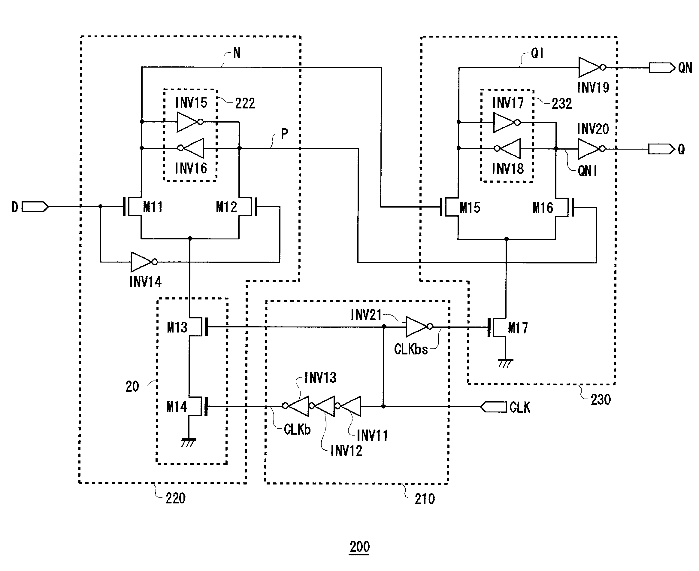
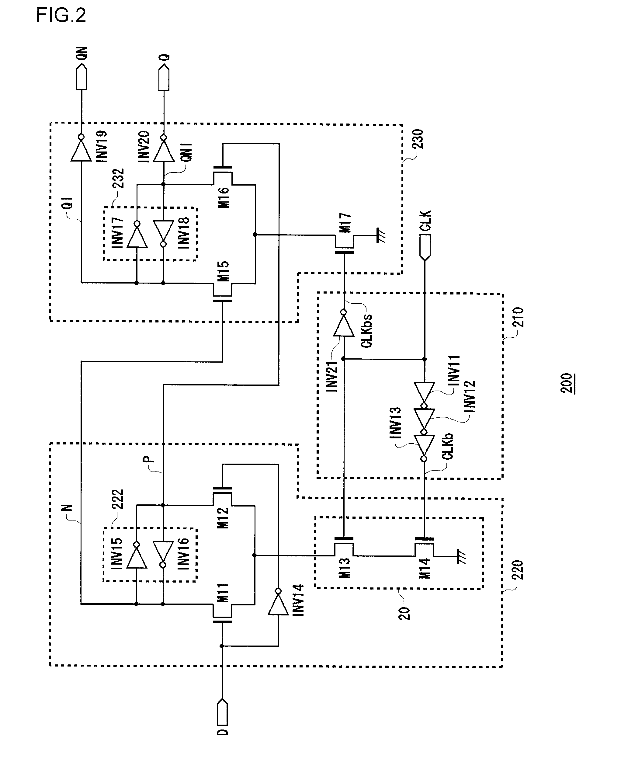
[0048]FIG. 2 is a circuit diagram of a flip-flop 200 according to a first embodiment of the present invention. A low-amplitude clock CLK and input data D are inputted to a flip-flop 200. The flip-flop 200 outputs output data Q and inverted output data QN. The low-amplitude clock CLK is a clock that oscillates at a voltage whose level is lower than a supply voltage. The flip-flop 200 takes in the input data D in synchronism with the low-amplitude clock CLK, outputs the thus taken-in data as the output data Q and outputs the inverted data thereof as inverted output data QN. The flip-flop 200 includes a clock control circuit 210, a master latch circuit 220 and a slave latch circuit 230.

[0049]The clock control circuit 210 includes an inverter INV 11, an inverter INV12 and an inverter INV13, which are connected in series to each other. An input terminal of the inverter INV13 is connected to the low-amplitude clock CLK. A voltage lower than a supply voltage is applied to the inverter INV1...

second embodiment

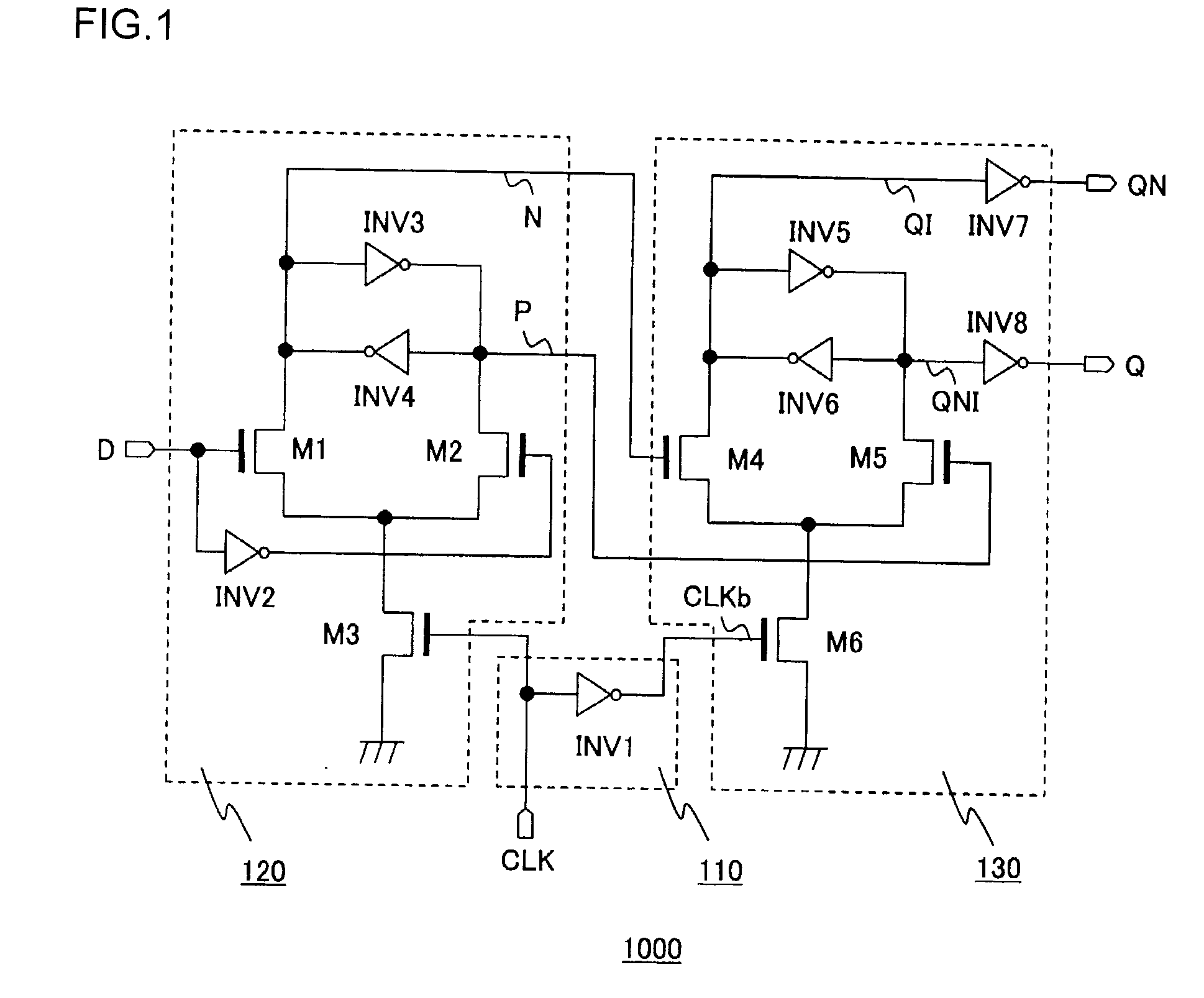
[0093]FIG. 7 is a circuit diagram showing a structure of a flip-flop circuit 100 according to a second embodiment of the present invention. As input / output terminals, the flip-flop circuit 100 includes an input terminal 102 to which input data D are inputted, an output terminal 104 from which an output signal Q is outputted, an inverted output terminal 106 from which an inverted output signal *Q is outputted, and a clock terminal 108 to which a clock signal CK is inputted. According to this second embodiment, the inversion of a given logical signal, namely its complementary level is denoted by*. This flip-flop circuit 100 latches the input data D based on the clock signal CK and then outputs the output signal Q and the inverted output signal *Q.

[0094]The flip-flop circuit 100 includes a latch circuit 10 and a clock control circuit 30.

[0095]The latch circuit 10 is a circuit for storing the input data D, and it includes a pair of transistors 12, an input inverter 14, internal inverter...


PUM


Abstract

A pair of transistors receive the input of signals of input data and the inverted input data. An activation circuit, which is provided between the pair of transistors and fixed potential, activates the pair of transistors in a conduction state. A clock control circuit receives a clock signal and sets the activation circuit to a conduction state for a predetermined period starting from an edge timing of the clock signal. The activation circuit includes a first activation transistor and a second activation transistor which are connected in cascade with each other. The clock control circuit turns on both the first activation transistor and the second transistor for the predetermined period starting from the edge timing of the clock signal, and turns off at least one of the first activation transistor and the second activation transistor for a period other than the predetermined period.

Description

BACKGROUND OF THE INVENTION[0001]1. Field of the Invention[0002]The present invention relates to a flip-flop circuit that latches inputted data.[0003]2. Description of the Related Art[0004]A reduction in power consumption is required for an LSI (Large Scale Integration) circuit mounted on battery-operated equipment represented by mobile devices. As described FIG. 2 in Reference (1) in the following Related Art List, 20% to 45% of power consumed in the an LSI circuit is consumed as power consumed by the charging and discharging of capacitance by clock signals. Thus, the reduction in power consumed by the charging and discharging will be effective.[0005]The power consumed by the charging and discharging of clock signals is proportional to the square of supply voltage. In this connection, to reduce the power consumed by the charging and discharging of clock signals, a method has been proposed where the supply voltage of a clock buffer is lowered and the amplitude of clock signals is re...

Claims


Application Information

Patent Timeline
Patent Type & Authority Applications(United States)
IPC IPC(8): H03K3/356H03K3/00
CPCH03K3/35625H03K3/356034
Inventor FURUICHI, SHINJISEKINE, SATORU
Owner SANYO ELECTRIC CO LTD
Learn More