Display device, method of driving same, and electonic device

a display device and active matrix technology, applied in static indicating devices, instruments, electroluminescent light sources, etc., can solve the problems of affecting the resolution improvement of the display device, the complexity of the pixel circuit, and the inability of the transistors to drive the light-emitting device to be uniform in threshold voltage and mobility, so as to achieve the effect of reducing the number of lines, reducing the pixel area, and high image quality

Active Publication Date: 2008-02-07
JOLED INC
View PDF3 Cites 85 Cited by
  • Summary
  • Abstract
  • Description
  • Claims
  • Application Information

AI Technical Summary

Benefits of technology

[0013]One embodiment of the present invention provides an active matrix display device using light-emitting devices such as organic electroluminescent devices (OEDs) at pixels. Each pixel has at least a function of correcting the threshold voltage for the driving transistor. Preferably, the pixel has the function of correcting the mobility of the driving transistor and the function of correcting for timewise variations in the characteristics of the OEDs (bootstrap operation). As a result, high image quality can be obtained. To incorporate these corrective functions, the power-supply voltage supplied to each pixel is used as a switching pulse. This eliminates switching transistors, which would normally be used to correct the threshold voltage, and scanning lines, which controls the gate of the switching transistors. As a result, the number of elements constituting the pixel circuit and the number of lines can be reduced greatly. Hence, the pixel area can be reduced. Consequently, higher resolution of the display can be accomplished. In the related-art pixel circuit having such corrective functions, there are many elements and so the layout area is large. Consequently, the related-art pixel circuit is unsuited for higher resolution of display devices. In one embodiment of the present invention, the number of the constituent elements and the number of lines are reduced by switching the power-supply voltage. The pixel layout area can be reduced. Thus, a high-quality, high-definition flat display can be offered.
[0014]In one embodiment of the present invention, the operation for correcting the threshold voltage is repeatedly performed in plural horizontal periods preceding sampling of the signal potential. This assures that a voltage corresponding to the threshold voltage for the driving transistor is retained in the retaining capacitor. In one embodiment of the invention, correction of the threshold voltage for the driving transistor is carried out by plural discrete operations and so the total time to correct the threshold voltage can be secured sufficiently. The voltage corresponding to the threshold voltage for the driving transistor can be reliably retained in the retaining capacitor previously. The voltage which is retained in the retaining capacitor and which corresponds to the threshold voltage is added to the signal potential similarly sampled and retained into the retaining capacitor. This is added to the gate of the driving transistor. The voltage which is added to the sampled signal potential and which corresponds to the threshold voltage just cancels the threshold voltage for the driving transistor. Therefore, a driving current corresponding to the signal potential can be supplied to the light-emitting devices without being affected by the variations. For this purpose, it is important that the voltage corresponding to the threshold voltage be retained in the retaining capacitor reliably. In one embodiment of the present invention, writing of the voltage corresponding to the threshold voltage is carried out by plural discrete repetitive operations. In this way, a time for the writing is secured sufficiently. Because of this configuration, brightness nonuniformity especially at low gray levels can be suppressed.

Problems solved by technology

However, in related-art active-matrix self-luminous flat panel displays, transistors for driving the light-emitting devices are not uniform in threshold voltage and mobility due to process variations.
That is, the pixel circuit is complex in configuration.
Improvement of the resolution of the display device is hindered by the fact that the pixel circuit is made up of a large number of components.

Method used


Image

  • Display device, method of driving same, and electonic device
  • Display device, method of driving same, and electonic device
  • Display device, method of driving same, and electonic device

Examples


Embodiment Construction

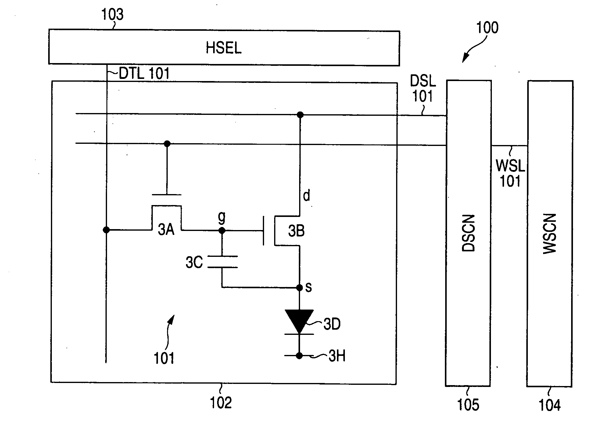
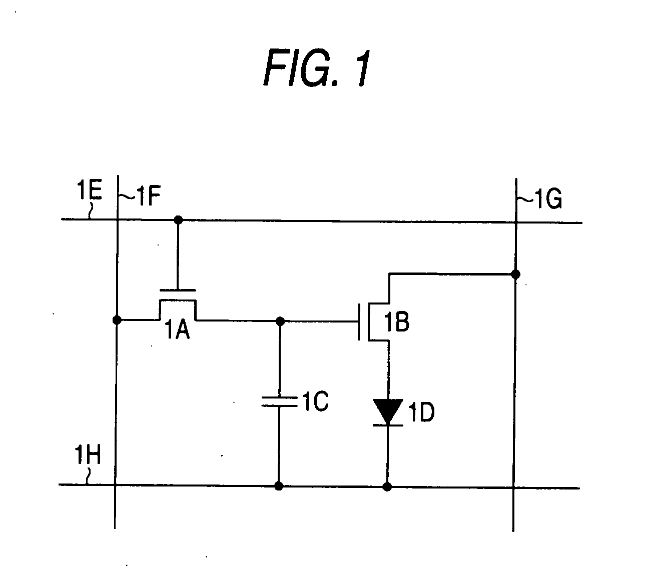
[0056]Embodiments of the present invention are hereinafter described in detail with reference to the drawings. To facilitate understanding the present invention and make clear the background of the invention, a general structure of a display device is briefly described by referring to FIG. 1. FIG. 1 is a schematic circuit diagram of one pixel of a general display device. As shown, in this pixel circuit, a transistor 1A for sampling is disposed at the intersection of a scanning line 1E and a signal line 1F which are orthogonal to each other. The transistor 1A is of the N type. The gate of the transistor is connected with the scanning line 1E, while the drain is connected with the signal line 1F. One electrode of a retaining capacitor 1C and the gate of a driving transistor 1B are connected with the source of the sampling transistor 1A. The driving transistor 1B is of the N type. A power-supply line 1G is connected with the drain of the driving transistor 1B. The anode of a light-emit...


PUM


Abstract

A display device is disclosed. The display device includes: a pixel array portion and a driver portion for driving the pixel array portion. The pixel array portion has rows of scanning lines, columns of signal lines, pixels arranged in rows and columns at intersections of the scanning lines and the signal lines, and power lines disposed in a corresponding manner to the rows of the pixels. The driver portion includes a main scanner, a power-supply scanner, and a signal selector. Each of the pixels includes light-emitting devices, a sampling transistor, a driving transistor, a retaining capacitor.

Description

CROSS REFERENCES TO RELATED APPLICATION[0001]The present invention contains subject matter related to Japanese Patent Application JP2006-209326 filed in the Japanese Patent Office on Aug. 1, 2006, the entire contents of which being incorporated herein by reference.BACKGROUND OF THE INVENTION[0002]1. Field of the Invention[0003]The present invention relates to an active matrix display device using light-emitting devices at pixels and also to a method of driving the display device. Furthermore, the invention relates to an electronic device incorporating such a display device.[0004]2. Description of the Related Art[0005]In recent years, self-luminous flat panel displays using organic electroluminescent devices (OEDs) as light-emitting devices have been developed vigorously. An OED is a device making use of the phenomenon that electroluminescence occurs when an electric field is applied to an organic thin film. Since OEDs are driven when a voltage of less than 10 V is applied, the devic...

Claims


Application Information

Patent Timeline
Patent Type & Authority Applications(United States)
IPC IPC(8): G09G3/30G09G5/00
CPCG09G3/3233G09G3/3266G09G2300/0819G09G2300/0842G09G2300/0866G09G3/20G09G3/30G09G3/32H05B33/12
Inventor IIDA, YUKIHITOUCHINO, KATSUHIDEYAMAMOTO, TETSURO
Owner JOLED INC
Why Eureka
Try Eureka