Semiconductor device with stacked chips and method for manufacturing thereof

a technology of semiconductors and stacked chips, applied in the direction of semiconductor/solid-state device manufacturing, solid-state devices, electric devices, etc., can solve the problem of low productivity of manufacturing process and manufacture process, and achieve the effect of improving manufacturing productivity

Inactive Publication Date: 2008-02-07
POLARIS INNOVATIONS LTD
View PDF8 Cites 52 Cited by
  • Summary
  • Abstract
  • Description
  • Claims
  • Application Information

AI Technical Summary

Benefits of technology

[0007]An exemplary embodiment of the present invention is directed to a method for manufacturing a semiconductor device with stacked chips, which improves the productivity of manufacturing.

Problems solved by technology

Therefore, the manufacturing process is made chip by chip with a low productivity.

Method used


Image

  • Semiconductor device with stacked chips and method for manufacturing thereof
  • Semiconductor device with stacked chips and method for manufacturing thereof
  • Semiconductor device with stacked chips and method for manufacturing thereof

Examples


Embodiment Construction

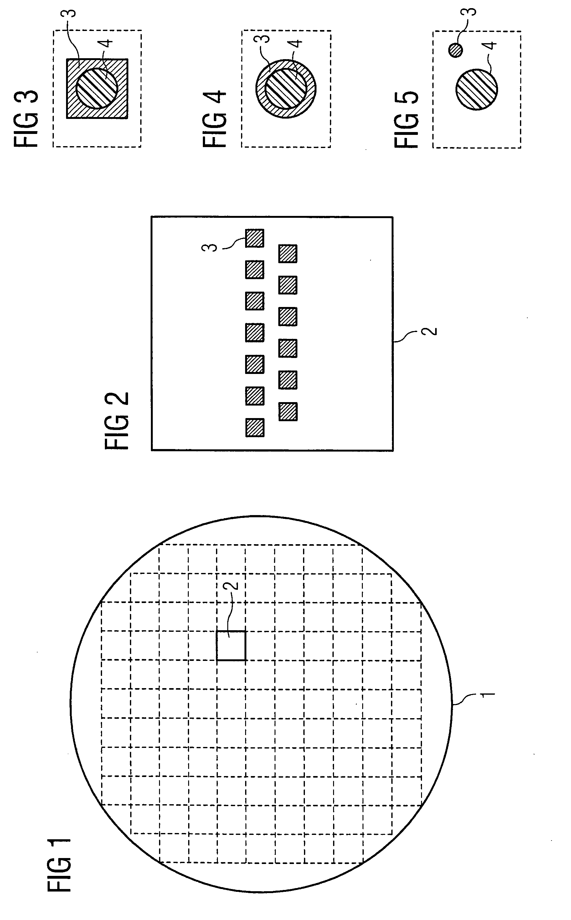
[0071]As shown in FIG. 1 a semiconductor wafer 1 generally contains multiple semiconductor chips 2. Each chip 2 comprises an electronic circuit (not shown). As shown in FIG. 2 contact pads 3 are arranged on the chip 2 for electrically connecting the electronic circuit with other electronic circuits or with a substrate.

[0072]At least some of the contact pads 3 are provided with an area 4 for through-hole silicon interconnects. This area 4 is intended for mounting a tower contact bump on a first semiconductor wafer or for placing a through-hole in a second semiconductor wafer as described in more detail below. FIG. 3 or FIG. 4 show different designs of contact pads 3. FIG. 3 shows the contact pad 3 in a square shape with a circular shaped area 4 in the center. FIG. 4 shows a circular shaped contact pad 3 with a co-centrically arranged circular shaped area 4.

[0073]FIG. 5 shows the case that the contact pad 3 and the area 4 are displaced. As described below the invention allows also in ...


PUM


Abstract

A semiconductor device includes a first semiconductor device and a second semiconductor device. Through-holes in the second semiconductor device extend from an upper side of the second semiconductor device adjacent contact pads to a bottom side of the second device. Tower contact bumps are electrically connected to contact pads of the first semiconductor device. The second semiconductor device is arranged adjacent the first semiconductor device so that the tower contact bumps are disposed within the through-holes and are electrically connected with contact pads of the second semiconductor device.

Description

TECHNICAL FIELD[0001]The present invention relates generally to semiconductor devices, and in a particular embodiment to a semiconductor device with stacked chips and a method of manufacturing the same.BACKGROUND[0002]To increase the functionality and density of semiconductor devices multiple semiconductor chips are stacked on a substrate or on each other. For instance, chips with the same functions, e.g., memory chips are stacked to increase the memory density or chips with different functions, e.g., processor chip and memory chip are stacked to minimize the processing time. Usually a first chip is mounted on a substrate. This chip is connected to substrate either by bonding bumps using flip-chip technology or by wire bonding. A second chip is then mounted onto the upper side of the first chip. In case of flip-chip bonding the second chip is mounted directly on the back side of the first chip (with an interlaying adhesive tape) or in case of wire bonding with spacers arranged betwe...

Claims


Application Information

Patent Timeline
Patent Type & Authority Applications(United States)
IPC IPC(8): H01L21/00
CPCH01L21/76898H01L2224/05554H01L24/06H01L24/11H01L24/12H01L24/16H01L24/83H01L24/90H01L25/0652H01L25/50H01L2224/0401H01L2224/04042H01L2224/0557H01L2224/06136H01L2224/13009H01L2224/13099H01L2224/13144H01L2224/13147H01L2224/16237H01L2224/2518H01L2224/83194H01L2224/838H01L2225/06541H01L2225/06593H01L2225/06596H01L2924/01002H01L2924/01004H01L2924/01014H01L2924/01027H01L2924/01029H01L2924/01033H01L2924/01075H01L2924/01078H01L2924/01079H01L2924/01082H01L2924/014H01L2924/05042H01L2224/16145H01L2224/9202H01L2924/01006H01L2224/16147H01L2224/81191H01L2224/81141H01L2224/9201H01L23/481H01L2224/16235H01L2224/02166
Inventor SIMON, JUERGENHEDLER, HARRY
Owner POLARIS INNOVATIONS LTD
Why Eureka
Try Eureka