Semiconductor optical device and manufacturing method therefor

a technology of semiconductors and optical devices, applied in semiconductor devices, lasers, semiconductor lasers, etc., can solve the problems of difficult to reduce the generation of these to zero, degrading the laser property, and difficult to reduce the production yield to zero, so as to prevent the damage of the layer, stable state, and high controllability

Inactive Publication Date: 2008-02-14
OPNEXT JAPAN INC
View PDF3 Cites 12 Cited by
  • Summary
  • Abstract
  • Description
  • Claims
  • Application Information

AI Technical Summary

Benefits of technology

[0015]The spacer layer is made of a material which can be selectively etched with respect to the second layer; the spacer layer is made of a material having a small selective ratio with respect to a third layer formed in contact with an upper surface of the first layer; and the damage receptor layer serves to prevent formation of the damaged layer in the second layer caused by the dry etching.
[0016]As described above, according to the present invention, the damaged layer abo...

Problems solved by technology

However, the following problems arise in cases where these methods are applied to post-treatment after dry etching of a passivation film located on an upper portion of a ridge waveguide structure.
This causes degradation of a laser property, which is not desirable as a post-treatment method.
Besides, by a removing method using wet etching, it is difficult to selectively remove only a d...

Method used


Image

  • Semiconductor optical device and manufacturing method therefor
  • Semiconductor optical device and manufacturing method therefor
  • Semiconductor optical device and manufacturing method therefor

Examples


Embodiment Construction

[0025]Hereinafter, embodiments of the present invention will be described with reference to the drawings. First, descriptions will be made of structures of semiconductor optical devices according to embodiments of the present invention, and then manufacturing methods thereof will be described.

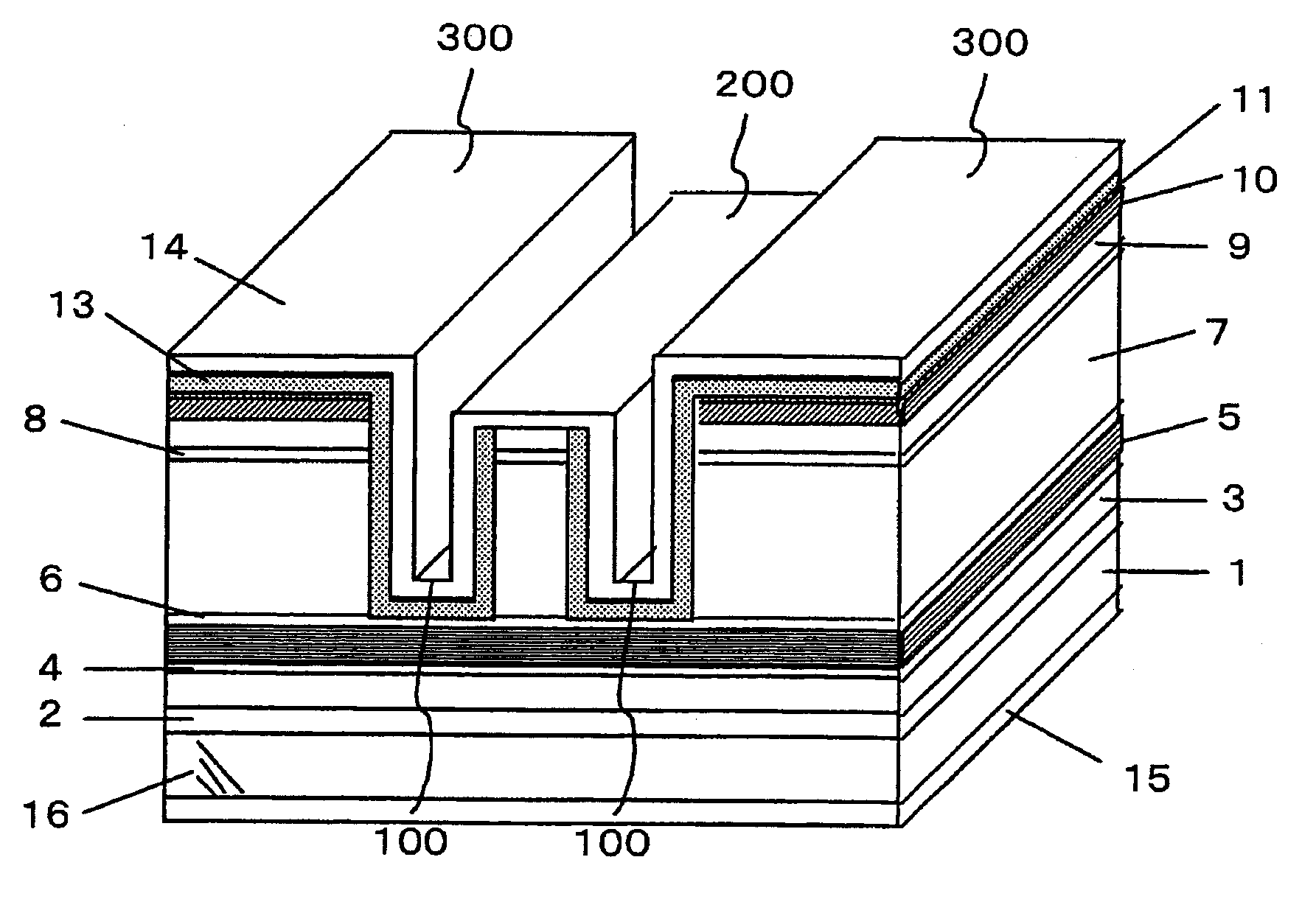
[0026]As shown in FIG. 6, a semiconductor optical device according to the present invention is an example applied to a semiconductor laser device of a ridge waveguide structure.

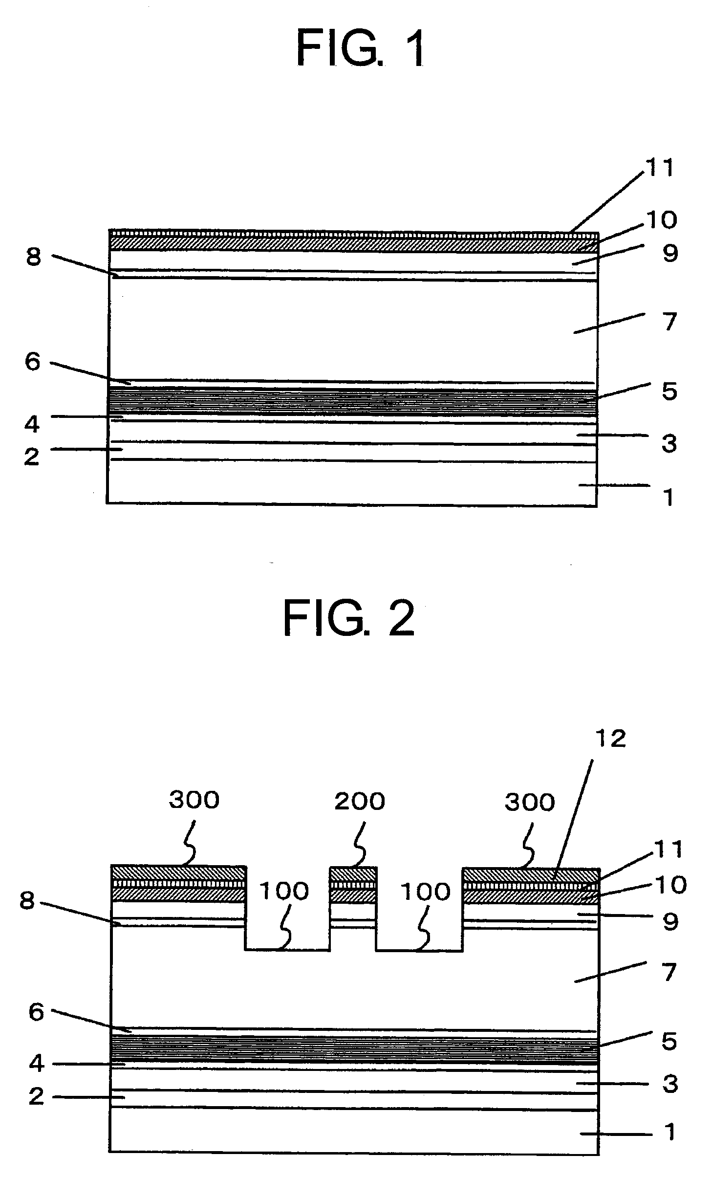
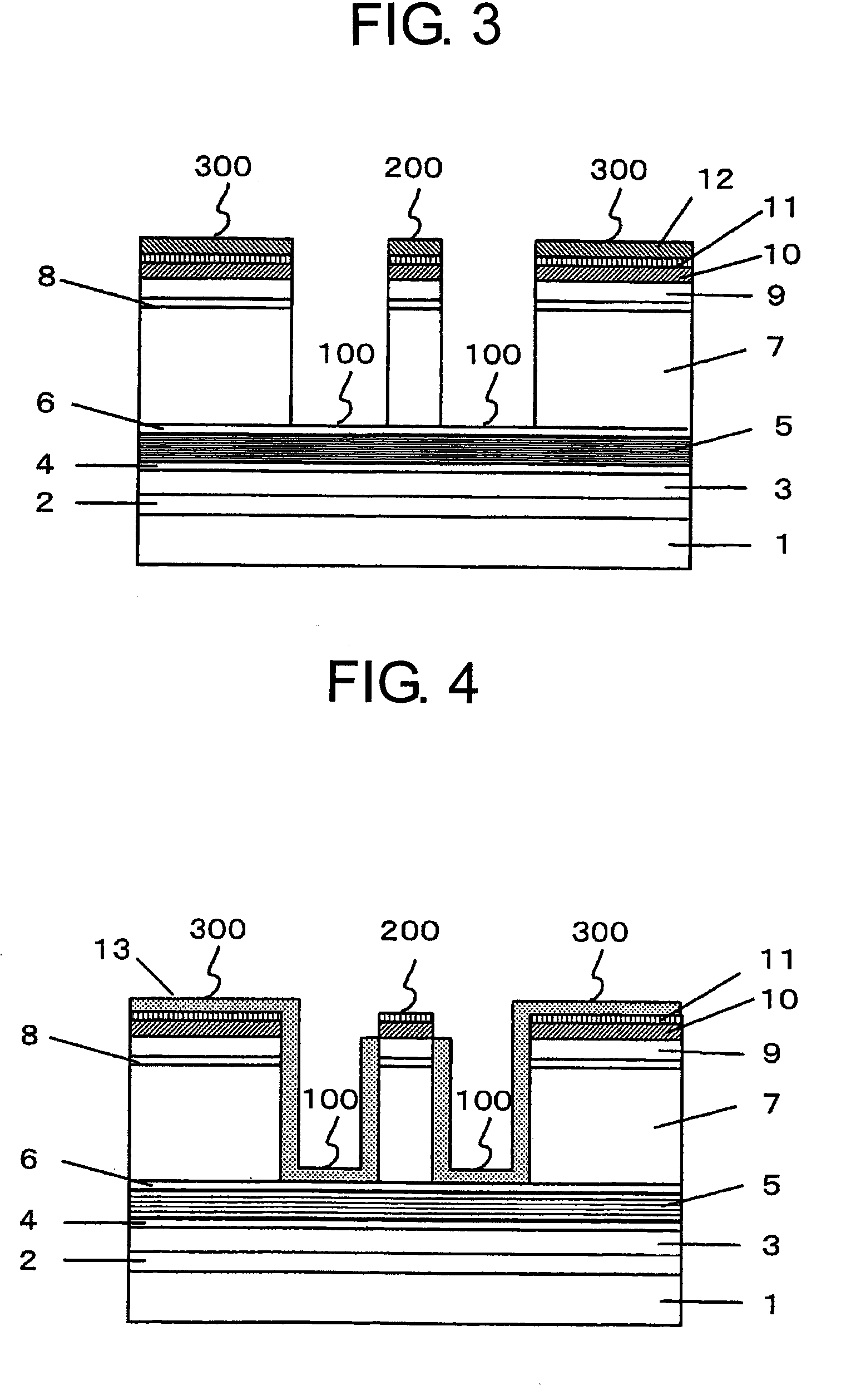
[0027]FIG. 6 shows a ridge waveguide type semiconductor laser according to the present invention. A buffer layer 2, a clad layer 3, a guide layer 4, a strained multiple quantum well active layer 5, a guide layer 6, a clad layer 7, a hetero barrier reducing layer 8, a contact layer 9, a spacer layer 10, and a damage receptor layer 11 are formed on a semiconductor substrate 1 in the stated order. Further, two grooves 100 are formed by engraving from an upper surface toward the semiconductor substrate 1 as deep as a locatio...


PUM


Abstract

To eliminate generation of a damaged layer caused by dry etching of a contact layer, occurring in a manufacturing process of a ridge waveguide type semiconductor laser, and to improve reliability and yield thereof, a method is provided involving forming a spacer layer and a damage receptor layer on the contact layer, making the two layer absorb damage caused by dry etching a passivation film in an upper portion of the ridge waveguide structure, and thereafter removing the damaged layer by the dry etching, by selective removal by wet etching.

Description

[0001]This application claims a priority from the Japanese Patent Application No. 2006-218341 filed on Aug. 10, 2006, the entire content of which is incorporated by reference herein.FIELD OF THE INVENTION[0002]The present invention relates to a semiconductor optical device and a manufacturing method therefor, and more particularly, to a technology which is effective when applied to a semiconductor laser device having a ridge waveguide structure.BACKGROUND OF THE INVENTION[0003]In general, in a semiconductor laser device, to attain an enhanced efficiency of current injection and to a control lateral mode thereof, a ridge waveguide structure is formed between a contact layer and a second clad layer. This ridge waveguide structure is referred to as a semiconductor mesa, and laser oscillation can be performed by injecting current to the contact layer on the semiconductor mesa.[0004]Hitherto, a process for forming a current injection region above the semiconductor mesa has involved remov...

Claims


Application Information

Patent Timeline
IPC IPC(8): H01L29/06H01L21/302B82Y20/00H01S5/042H01S5/22
CPCH01S5/0425H01S5/2086H01S2301/173H01S5/22H01S5/209H01S2301/176H01S5/04254
Inventor SAKUMA, YASUSHIKOMATSU, KAZUHIROHAYAKAWA, SHIGENORINAKAI, DAISUKE
Owner OPNEXT JAPAN INC
Why Eureka
Try Eureka