Semiconductor Device

a technology of semiconductors and devices, applied in the field of semiconductor devices, can solve the problem that data cannot be additionally written, and achieve the effect of high function and high added valu

Inactive Publication Date: 2008-02-21
SEMICON ENERGY LAB CO LTD
View PDF12 Cites 52 Cited by
  • Summary
  • Abstract
  • Description
  • Claims
  • Application Information

AI Technical Summary

Benefits of technology

[0027] Therefore, a semiconductor device in which high function and high a

Problems solved by technology

A mask ROM has a simple structure, however, data is required to be written d

Method used


Image

  • Semiconductor Device
  • Semiconductor Device
  • Semiconductor Device

Examples


embodiment mode 1

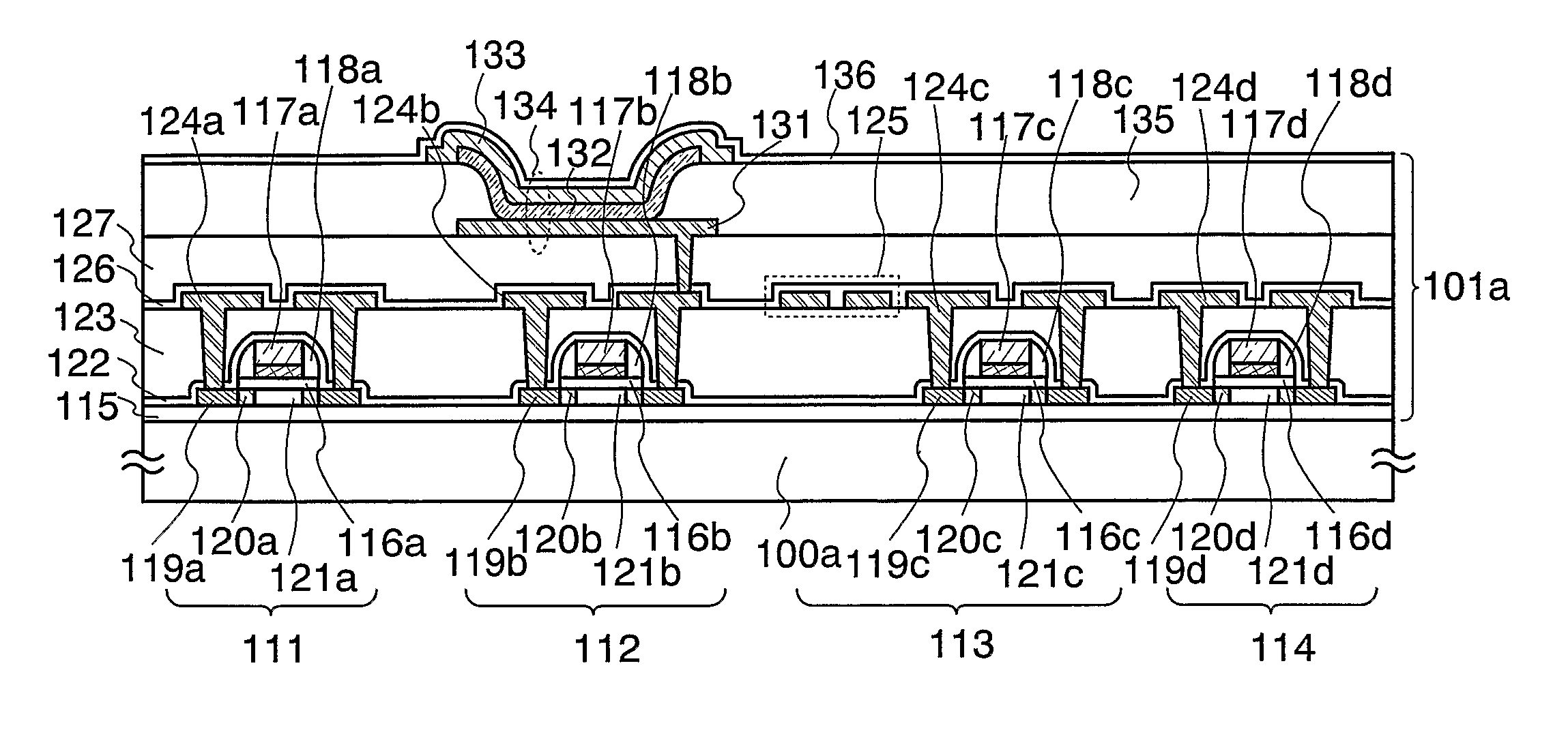
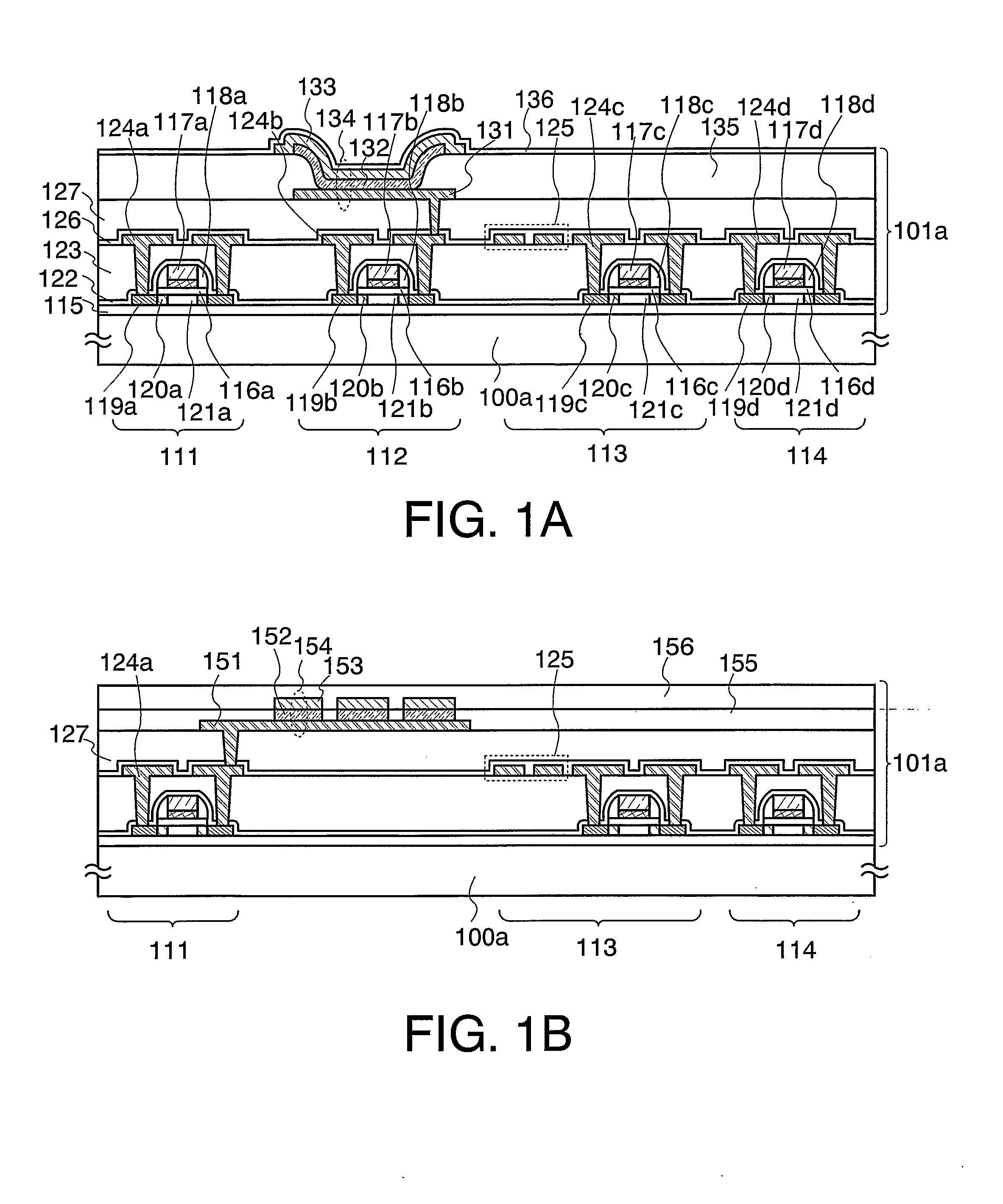
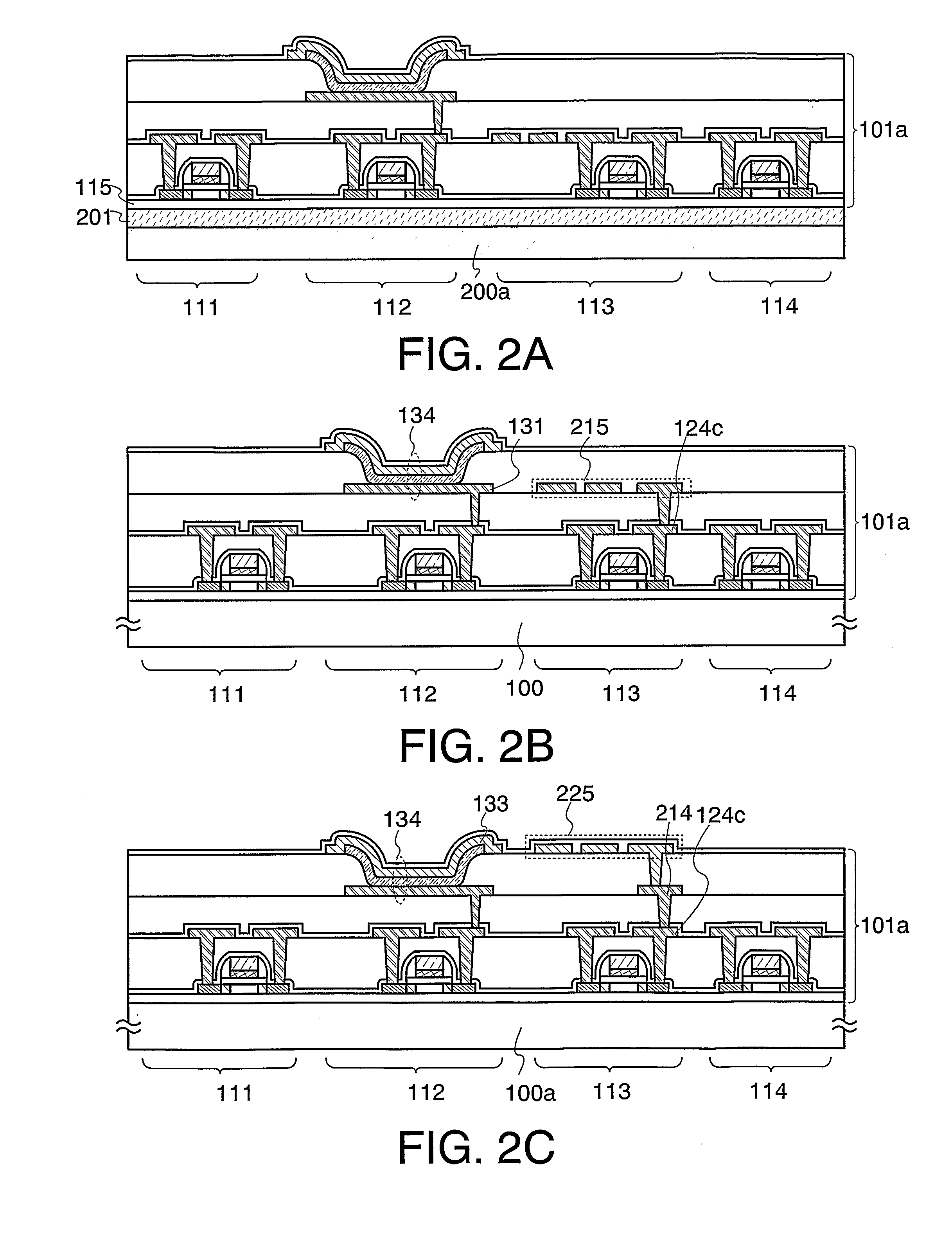
[0066] Description is made with reference to FIGS. 1A and 1B, 2A-2C, and 7A, and 15 on structures of semiconductor devices of this embodiment mode. As shown in FIG. 15, a semiconductor device 20 of the invention has a function to communicate data without contact and includes a power source circuit 11, a clock generating circuit 12, a data demodulation / modulation circuit 13, a control circuit 14 which controls other circuits, an interface circuit 15, a memory circuit 16, a data bus 17, and an antenna (antenna coil) 18.

[0067] The power source circuit 11 generates various power sources to be supplied to each circuit of the semiconductor device 20 based on an AC signal input from the antenna 18. The clock generating circuit 12 generates various clock signals to be supplied to each circuit of the semiconductor device 20 based on an AC signal input from the antenna 18. The data demodulation / modulation circuit 13 has a function to demodulate / modulate data to communicate with a reader / writ...

embodiment mode 2

[0106] In this embodiment mode, description is made with reference to FIGS. 3A, 3B, 7B, and 37 on structures of semiconductor devices of the invention, which are different than in the aforementioned embodiment mode.

[0107] As shown in FIG. 7B, a semiconductor device of this embodiment mode has a structure in which an element forming layer 301a including a plurality of transistors formed over the first substrate 100a and an element forming layer 302a including the conductive layer 105 which functions as an antenna formed over a second substrate 300a are attached by an adhesive layer.

[0108] Here, the element forming layer 301a including the plurality of transistors is typically formed of the regions 102 and 103 each of which includes a plurality of TFTs and the region 104 including a memory element. Further, the conductive layer 105 which functions as an antenna formed in the element forming layer 302a is connected to the region 102 including a plurality of TFTs which form a communic...

embodiment mode 3

[0120] In this embodiment mode, description is made with reference to FIGS. 4A, 4B, and 7C, 8A, and 8B on a sectional structure of a semiconductor device of the invention with a different structure than in the aforementioned embodiment modes. More specifically, description is made on a sectional structure of a semiconductor device with a structure in which a substrate over which an element forming layer 402a including a memory element is formed instead of a conductive layer which functions as an antenna in FIGS. 3A and 3B is attached.

[0121] A semiconductor device of this embodiment mode has a structure in which an element forming layer 401a including a plurality of transistors formed over the first substrate 100a, and an element forming layer 402a including a memory element formed over the second substrate 400a are attached by an adhesive layer.

[0122] Here, the element forming layer 401a including a plurality of transistors typically includes the regions 102 and 103 each of which ...


PUM


Abstract

The invention provides a semiconductor device which is non-volatile, easily manufactured, and can be additionally written. A semiconductor device of the invention includes a plurality of transistors, a conductive layer which functions as a source wiring or a drain wiring of the transistors, and a memory element which overlaps one of the plurality of transistors, and a conductive layer which functions as an antenna. The memory element includes a first conductive layer, an organic compound layer and a phase change layer, and a second conductive layer stacked in this order. The conductive layer which functions as an antenna and a conductive layer which functions as a source wiring or a drain wiring of the plurality of transistors are provided on the same layer.

Description

TECHNICAL FIELD [0001] The invention relates to a semiconductor device capable of data transmission / reception and a manufacturing method thereof. BACKGROUND ART [0002] In recent years, a semiconductor device having various functions and a plurality of circuits over an insulating surface has been developed. Further, development of a semiconductor device capable of wireless data transmission / reception by a provided antenna has been advanced. Such a semiconductor device, which is referred to as a wireless chip (referred to as ID tag, IC tag, IC chip, RF (Radio Frequency) tag, wireless tag, and electronic tag, and RFID (Radio Frequency Identification)), is already introduced to a part of the market. DISCLOSURE OF INVENTION [0003] By providing a memory circuit (also simply referred to as a memory) which stores data as various circuits integrated over a substrate, a semiconductor device having higher function and added value can be provided. As a memory circuit, a DRAM (Dynamic Random Acc...

Claims


Application Information

Patent Timeline
IPC IPC(8): H01L27/108
CPCB82Y10/00H01L27/1266G11C13/0004G11C13/0014G11C13/0016G11C13/0069G11C17/143G11C17/16G11C17/18G11C2013/009G11C2213/77G11C2213/79H01L21/8221H01L27/0688H01L27/2409H01L27/2436H01L27/2463H01L45/06H01L45/065H01L45/1213H01L45/1233H01L45/141H01L45/143H01L45/144G11C13/00H01L2224/48091H01L2224/48137H01L2224/49107H01L2224/73265H01L2924/12044H10B63/20H10B63/30H10B63/80H10N70/231H10N70/257H10N70/826H10N70/882H10N70/8825H10N70/8828H01L2924/00014H01L2924/00H01L29/78645H10N70/235H10K19/10H10K30/671H01L23/66H01L2223/6677
Inventor YAMAZAKI, SHUNPEIABE, HIROKONEMOTO, YUKIENOMURA, RYOJIYUKAWA, MIKIO
Owner SEMICON ENERGY LAB CO LTD
Why Eureka
Try Eureka