Image Sensor and Method for Manufacturing the Same

a technology of image sensor and manufacturing method, which is applied in the direction of solid-state devices, semiconductor devices, radio frequency controlled devices, etc., can solve the problems of low sensitivity or saturation level, image lagging, and inability to properly achieve pining, so as to achieve the effect of maximizing the depletion of photodiodes

Inactive Publication Date: 2008-02-21
DONGBU HITEK CO LTD
View PDF1 Cites 5 Cited by
  • Summary
  • Abstract
  • Description
  • Claims
  • Application Information

AI Technical Summary

Benefits of technology

[0007]Embodiments of the present invention provide an image sensor and a method for manufacturing the same, which incorporates implanting ions into an N-type ion imp...

Problems solved by technology

However, according to the related art, when the pinning is not completely made, the depletion area where the electrons are generated becomes narrow so that sensitivity or saturation level becomes low.
In addition, when the reset is not completely made, image lagging occurs.
In other words, with the image sensor according to...

Method used


Image

  • Image Sensor and Method for Manufacturing the Same
  • Image Sensor and Method for Manufacturing the Same
  • Image Sensor and Method for Manufacturing the Same

Examples


first embodiment

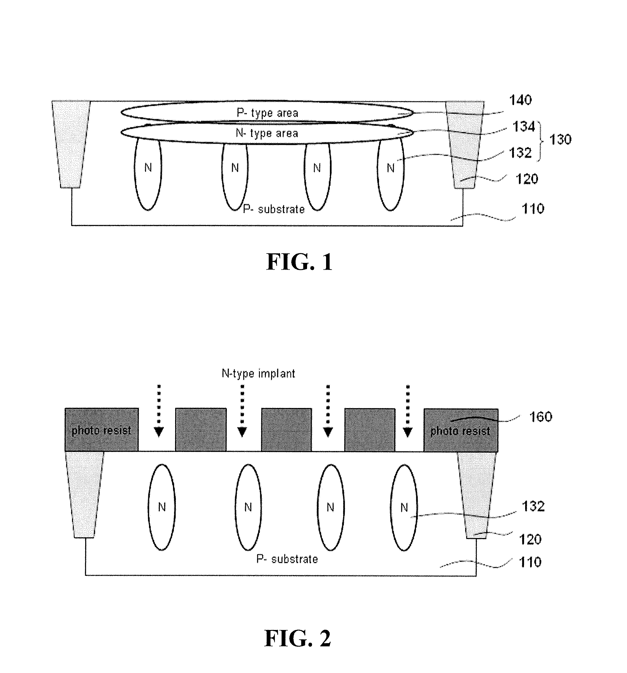
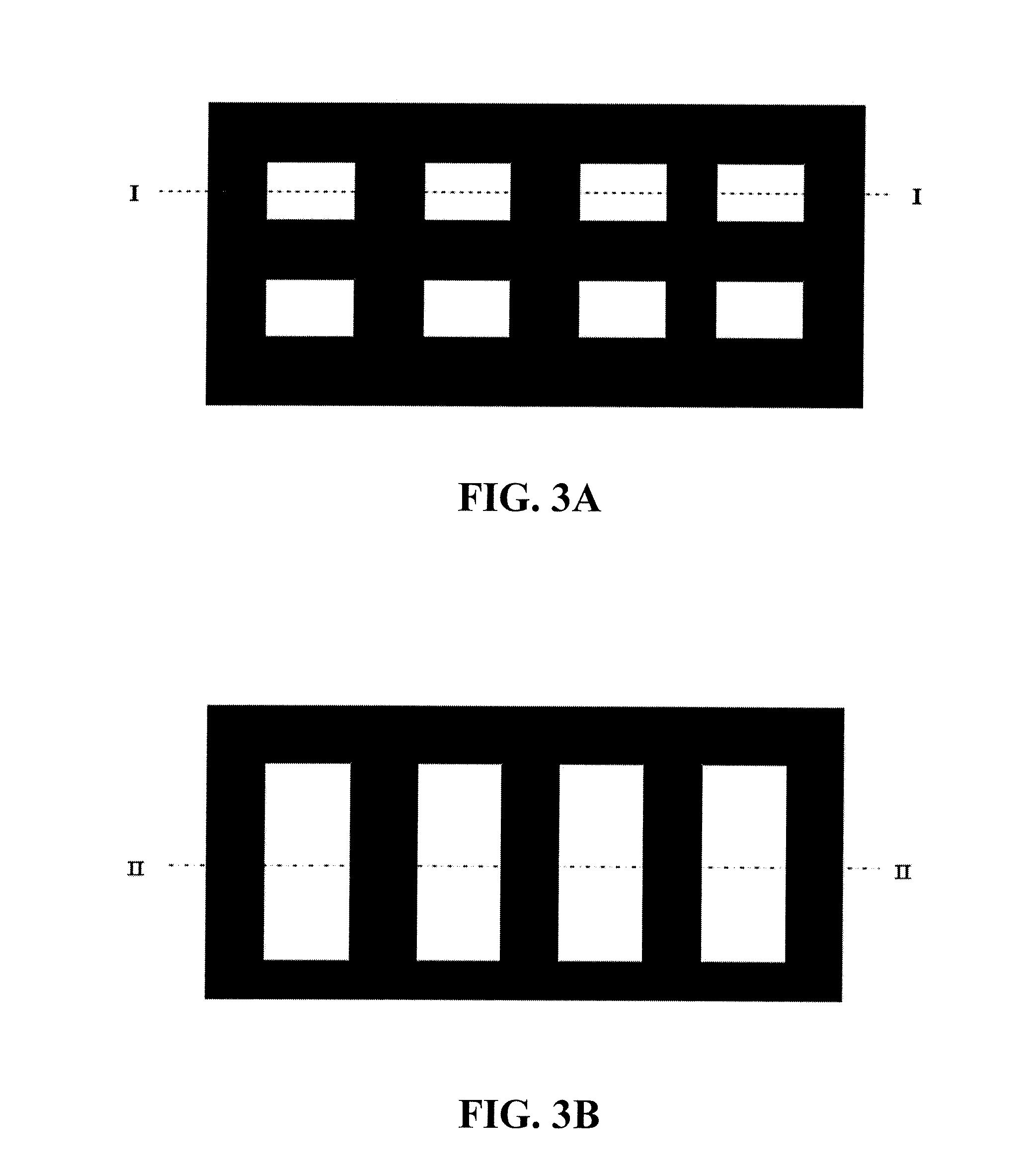
[0034]FIGS. 2, 4 and 5 are cross-sectional views showing the manufacturing process of an image sensor according to a first embodiment.

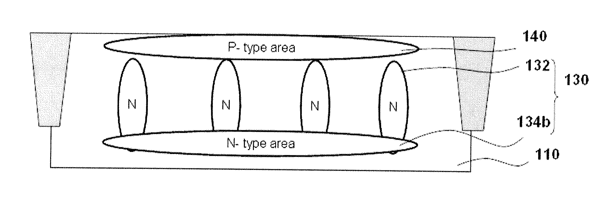
[0035]The method for manufacturing the image sensor according to a first embodiment includes: defining an active area; forming a second conductive type first ion implant area; forming a second conductive type second ion implant area; and forming a first conductive type ion implant area.

[0036]The method for manufacturing the image sensor as described below involves a P-type semiconductor substrate, an N-type first and second ion implant area, and a P-type ion implant area, but embodiments are not limited thereto.

[0037]Referring to FIG. 2, an active area can be defined by forming a device isolation layer 120 on a first conductive type semiconductor substrate 110. The first conductive type semiconductor substrate 110 can be a P-type semiconductor substrate. In an embodiment, the first conductive type semiconductor substrate 110 can be made by forming a P...

second embodiment

[0053]FIG. 7 is a cross-sectional view showing depletion of an image sensor according to a second embodiment.

[0054]The method for manufacturing the image sensor according to a second embodiment includes: defining an active area; forming a second conductive type first ion implant area; forming a second conductive type second ion implant area; and forming a first conductive type ion implant area.

[0055]The method for manufacturing the image sensor according to the second embodiment can adopt some features of the first embodiment.

[0056]According to the second embodiment, the second conductive type first ion implant 232 can be formed to a depth of 9,000 to 11,000 Å from the surface of the first conductive type semiconductor substrate 110.

[0057]The second conductive type first ion implant area 232 can be formed by implanting ions with an implantation energy of 80 to 800 KeV. In one embodiment, the ion implant begins using an implantation energy of 80 KeV and then the implantation energy i...


PUM


Abstract

An image sensor is provided incorporating a first conductive type semiconductor substrate including an active area defined by a device isolation layer; a second conductive type first ion implant area formed as multiple regions in the active area; a second conductive type second ion implant area connecting the multiple regions of the second conductive type first ion implant area; and a first conductive type ion implant area formed on the second conductive type second ion implant area. The multiple regions of the second conductive type first ion implant area can be formed deeply in the substrate. The second conductive type second ion implant can be formed in the substrate at an upper region of the first ion implant area, a middle region of the first ion implant area, or a lower region of the first ion implant area.

Description

CROSS-REFERENCE TO RELATED APPLICATION[0001]The present application claims the benefit under 35 U.S.C. §119 of Korean Patent Application No. 10-2006-0078127, filed Aug. 18, 2006, which is hereby incorporated by reference in its entirety.BACKGROUND[0002]Generally, an image sensor is a semiconductor device that converts an optical image into an electrical signal. The image sensor is typically classified as a charge coupled device (CCD) image sensor or a Complementary Metal Oxide Silicon (CMOS) image sensor.[0003]The CMOS image sensor utilizes a photodiode and transistors to convert an optical image into an electrical signal. Light incident on a photodiode generates electrons in a depletion area of the photodiode, and signals can be generated using the electrons.[0004]The electrons generated in the depletion area are extracted from the photodiode through a reset process, and at this time, the whole of the photodiode should be depleted for resetting. This depletion is called being pinne...

Claims


Application Information

Patent Timeline
IPC IPC(8): H01L31/00H01L21/425
CPCH01L27/14643H01L27/14689Y02E10/50H01L31/103H01L31/03529H01L27/146
Inventor LIM, KEUN HYUK
Owner DONGBU HITEK CO LTD
Why Eureka
Try Eureka