Vertical gallium nitride-based light emitting diode and method of manufacturing the same
Active Publication Date: 2008-02-28
SAMSUNG ELECTRONICS CO LTD
View PDF14 Cites 141 Cited by
Summary
Abstract
Description
Claims
Application Information
AI Technical Summary
This helps you quickly interpret patents by identifying the three key elements:
Problems solved by technology
Method used
Benefits of technology
Benefits of technology
[0025]An advantage of the present invention is that it provides a vertical GaN-based LED and a method of manufacturing the same in which facilitates a dicing or scribing process for separating LEDs and prevents an overall structure including a structure support layer from being bent or short-circuited, thereby enhancing the reliability of an LED.
[0026]Another advantage of the invention is that it provides a vertical GaN-based LED and a method of manufacturing the same which can enhance the reliability of an LED by reducing a piezoelectric effect caused by a reflecting electrode which is formed on a p-type GaN-based semiconductor layer.
[0027]Additional aspect and advantages of the present general inventive concept will be set forth in part in the description which follows and, in part, will be obvious from the description, or may be learned by practice of the general inventive concept.
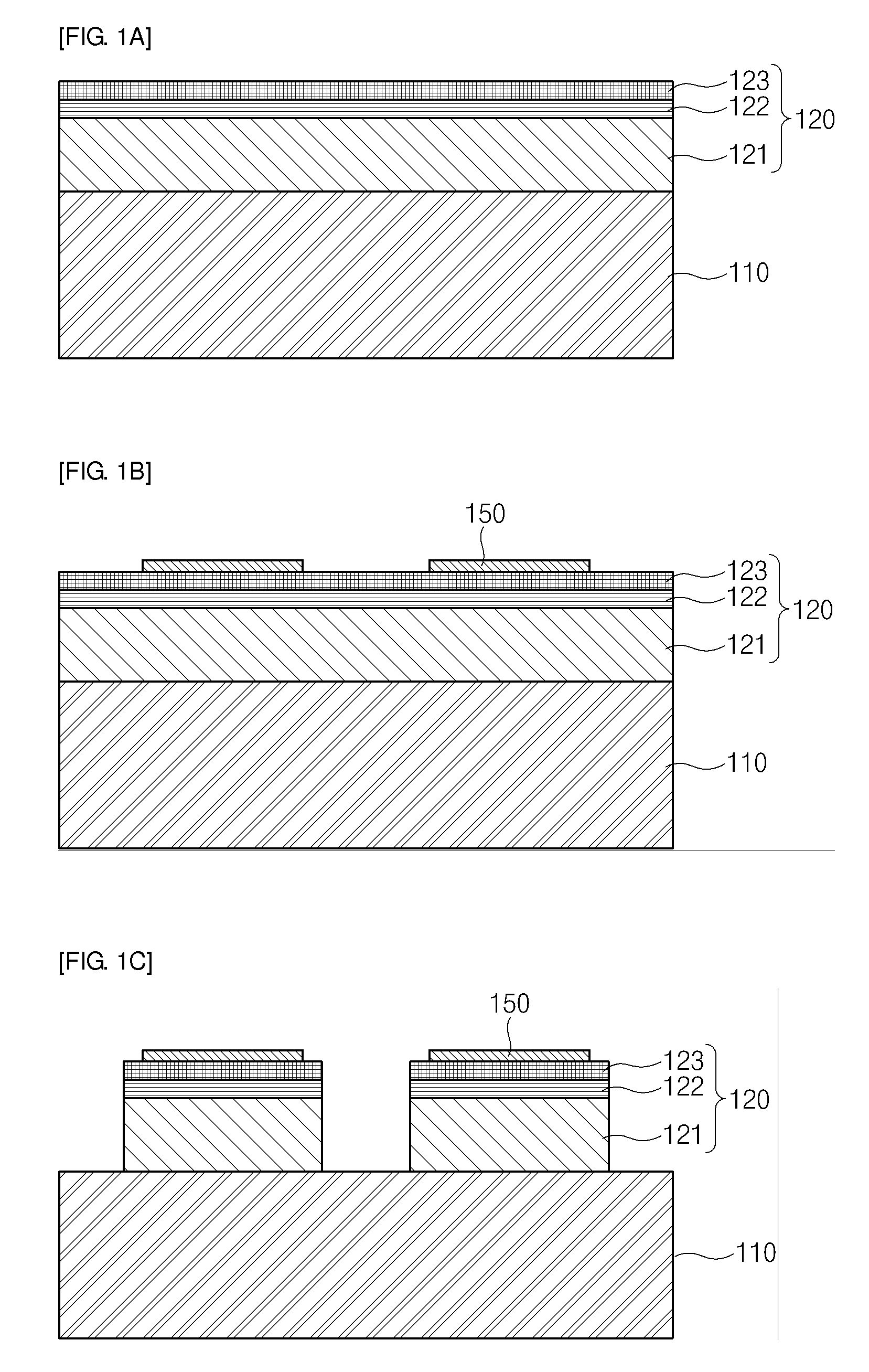
[0028]According to an aspect of the invention, a GaN-based LED comprises an n-electrode; a light emission structure formed under the n-electrode; a protective film formed on the outer surface of the light emission structure; a p-electrode formed under the light emission structure where the protective film is formed; a metal seed layer formed on the light emission structure and the entire surface of the p-electrode; and a conductive substrate formed under the metal seed layer.
[0029]Preferably, the light emission structure includes an n-type GaN-based semiconductor layer, an active layer, and a p-type GaN-based semiconductor layer.
[0030]Preferably, the n-type GaN-based semiconductor layer has surface irregularities formed on the upper surface thereof. The GaN-based LED further comprises a current blocking layer formed in the central portion of the lower surface of the light emission structure.
Therefore, there is a limitation in reducing the manufacturing costs by decreasing the size of a nitride-based semiconductor LED, or improving the optical power and chip characteristic.
However, while the dicing or laser scribing of the structure support layer 170 having a relatively large thickness is performed, the light emission structure 120 may be broken or damaged.
Therefore, it is not easy to perform a subsequent process.
As described above, when a vertical GaN-based LED is manufactured according to the related art, the reliability of the vertical GaN-based LED is degraded due to the above-described problems.
Therefore, a piezoelectric effect occurs so that the reliability of the LED is degraded.
Method used
Image
Click on the blue label to locate the original text in one second.
Reading with bidirectional positioning of images and text.
Examples
first embodiment
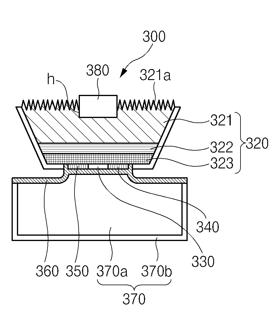
[0058]Referring to FIGS. 3 and 4A to 4M, a vertical GaN-based LED and a method of manufacturing the same according to a first embodiment will be described in detail.
[0059]FIG. 3 is a sectional view illustrating the structure of a vertical GaN-based LED according to the first embodiment of the invention. FIGS. 4A to 4M are sectional views sequentially showing a method of manufacturing a vertical GaN-based LED according to the first embodiment of the invention.
[0060]As shown in FIG. 4A, a light emission structure 320 is formed on a substrate 310, the light emission structure 320 being composed of a GaN-based semiconductor layer. In the light emission structure 320, an n-type GaN-based semiconductor layer 321, an active layer 322 composed of a GaN / InGaN layer with a multi-quantum well structure, and a p-type GaN-based semiconductor layer 323 are sequentially laminated.
[0061]Preferably, the substrate 310 is formed of a transparent material including sapphire. In addition to sapphire, th...
second embodiment
[0089]
[0090]Referring to FIGS. 5 to 8, a vertical GaN-based LED according to a second embodiment of the invention will be described in detail.
[0091]FIG. 5 is a sectional view of a vertical GaN-based LED according to the second embodiment of the invention. FIGS. 6 to 8 are plan views showing the shape of a reflecting electrode according to the invention.
[0092]As shown in FIG. 5, the vertical GaN-based LED 400 according to the second embodiment has an n-electrode 410 formed in the uppermost portion thereof.
[0093]Under the n-electrode 410, an n-type GaN-based semiconductor layer 420 is formed. More specifically, the n-type GaN-based semiconductor layer 420 may be formed of a GaN layer or GaN / AlGaN layer doped with n-type impurities.
[0094]In order to enhance a current spreading effect, a transparent electrode (not shown) is further formed between the n-electrode 410 and the n-type GaN-based semiconductor layer 420.
[0095]Under the n-type GaN-based semiconductor layer 420, an active layer...
third embodiment
[0115]
[0116]Now, a third embodiment of the invention will be described with reference to FIGS. 10 to 12. The descriptions of the same portions as those of the second embodiment will be omitted.
[0117]FIGS. 10 to 12 are sectional views illustrating the structure of a vertical GaN-based LED according to the third embodiment of the invention.
[0118]As shown in FIGS. 10 to 12, the vertical GaN-based LED according to the third embodiment has almost the same construction as the vertical GaN-based LED according to the second embodiment. However, the vertical GaN-based LED according to the third embodiment is different from the vertical GaN-based LED according to the second embodiment in that the barrier layer 455 is formed of an insulating film such that a portion of the reflecting electrode is formed to be exposed. The insulating film may be formed of an oxide-based or nitride-based material such as SiO2, Al2O3, TiO2, ZrO, HfO, SiN, AlN or the like.
PUM
Abstract
A method of manufacturing a vertical GaN-based LED comprises forming a light emission structure in which an n-type GaN-based semiconductor layer, an active layer, and a p-type GaN-based semiconductor layer are sequentially laminated on a substrate; etching the light emission structure such that the light emission structure is divided into units of LED; forming a p-electrode on each of the divided light emission structures; filling a non-conductive material between the divided light emission structures; forming a metal seed layer on the resulting structure; forming a first plated layer on the metal seed layer excluding a region between the light emission structures; forming a second plated layer on the metal seed layer between the first plated layers; separating the substrate from the light emission structures; removing the non-conductive material between the light emission structures exposed by separating the substrate; forming an n-electrode on the n-type GaN-based semiconductor layer; and removing portions of the metal seed layer and the second plated layer between the light emission structures.
Description
CROSS-REFERENCE TO RELATED APPLICATIONS[0001]This application claims the benefit of Korean Patent Application No. 10-2006-0079703 filed with the Korean Intellectual Property Office on Aug. 23, 2006 and Korean Patent Application No. 10-2007-0017519 filed with the Korean Intellectual Property Office on Feb. 21, 2007, the disclosure of which is incorporated herein by reference.BACKGROUND OF THE INVENTION[0002]1. Field of the Invention[0003]The present invention relates to a vertical galliumnitride-based light emitting diode (hereinafter, referred to as ‘a vertical GaN-based LED’) and a method of manufacturing the same, which can enhance reliability of an LED.[0004]2. Description of the Related Art[0005]Generally, a nitride-based semiconductor LED is grown on a sapphire substrate, but the sapphire substrate is a rigid nonconductor and has poor thermal conductivity. Therefore, there is a limitation in reducing the manufacturing costs by decreasing the size of a nitride-based semiconduct...
Claims
Application Information
Patent Timeline
Application Date:The date an application was filed.
Publication Date:The date a patent or application was officially published.
First Publication Date:The earliest publication date of a patent with the same application number.
Issue Date:Publication date of the patent grant document.
PCT Entry Date:The Entry date of PCT National Phase.
Estimated Expiry Date:The statutory expiry date of a patent right according to the Patent Law, and it is the longest term of protection that the patent right can achieve without the termination of the patent right due to other reasons(Term extension factor has been taken into account ).
Invalid Date:Actual expiry date is based on effective date or publication date of legal transaction data of invalid patent.

