Method of forming pattern of inorganic material film and structure containing the pattern

Active Publication Date: 2008-02-28
FUJIFILM CORP
View PDF0 Cites 11 Cited by
  • Summary
  • Abstract
  • Description
  • Claims
  • Application Information

AI Technical Summary

Benefits of technology

[0013]According to the present invention, cracks are produced by utilizing a difference between the thermal expansion coefficients of the sacrifice layer and the inorganic material layer formed thereon when the temperature of the substrate on which the sacrifice layer and the inorganic material

Problems solved by technology

However, conventionally, for functional films having a thickness of about 5 μm or more, there are not many appropriate fine patterning methods and appropriate materials to be employed therein.
For example, the etching method or the ion beam method has disadvantages that the substrate and surrounding elements are damaged, the process time is long, and the manufacturing cost is high, and therefore, the application to pattern-forming of the functional film is not so practical.
Further, although the liftoff method is higher in general versatility because the material dependence is lower than that of the etching method, the photoresist generally used as a sacrifice layer in the liftoff method deforms or burns dry at about 150° C., and the method is not applicable to the case where the process temperature (deposition temperature) becomes higher then 150° C.
However, the hydrofluoric acid used when removing silicon oxide and the acid or

Method used


Image

  • Method of forming pattern of inorganic material film and structure containing the pattern
  • Method of forming pattern of inorganic material film and structure containing the pattern
  • Method of forming pattern of inorganic material film and structure containing the pattern

Examples


Embodiment Construction

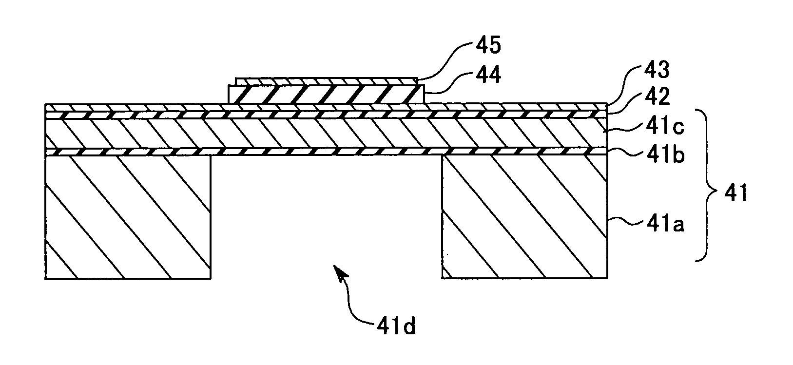
[0019]Hereinafter, preferred embodiments of the present invention will be explained in detail by referring to the drawings. The same reference numerals are assigned to the same component elements and the description thereof will be omitted.

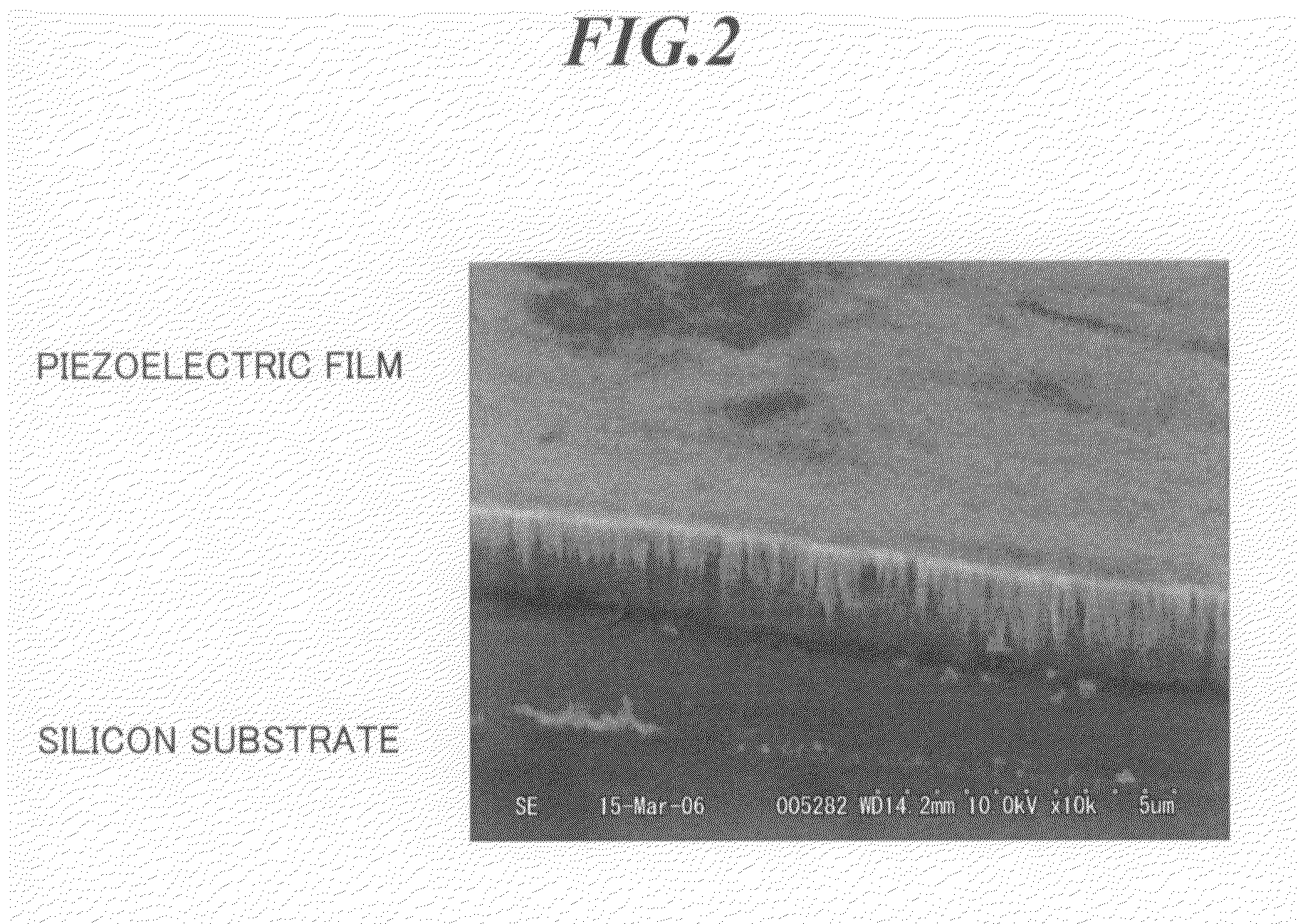
[0020]In this application, a material forming a main part, that exerts a function of an element (a multilayered capacitor, a piezoelectric element, etc.), such as a dielectric film, a piezoelectric film, and so on is referred to as a material having functionality or simply as a functional material. Further, a film formed of a functional material is referred to as a functional film.

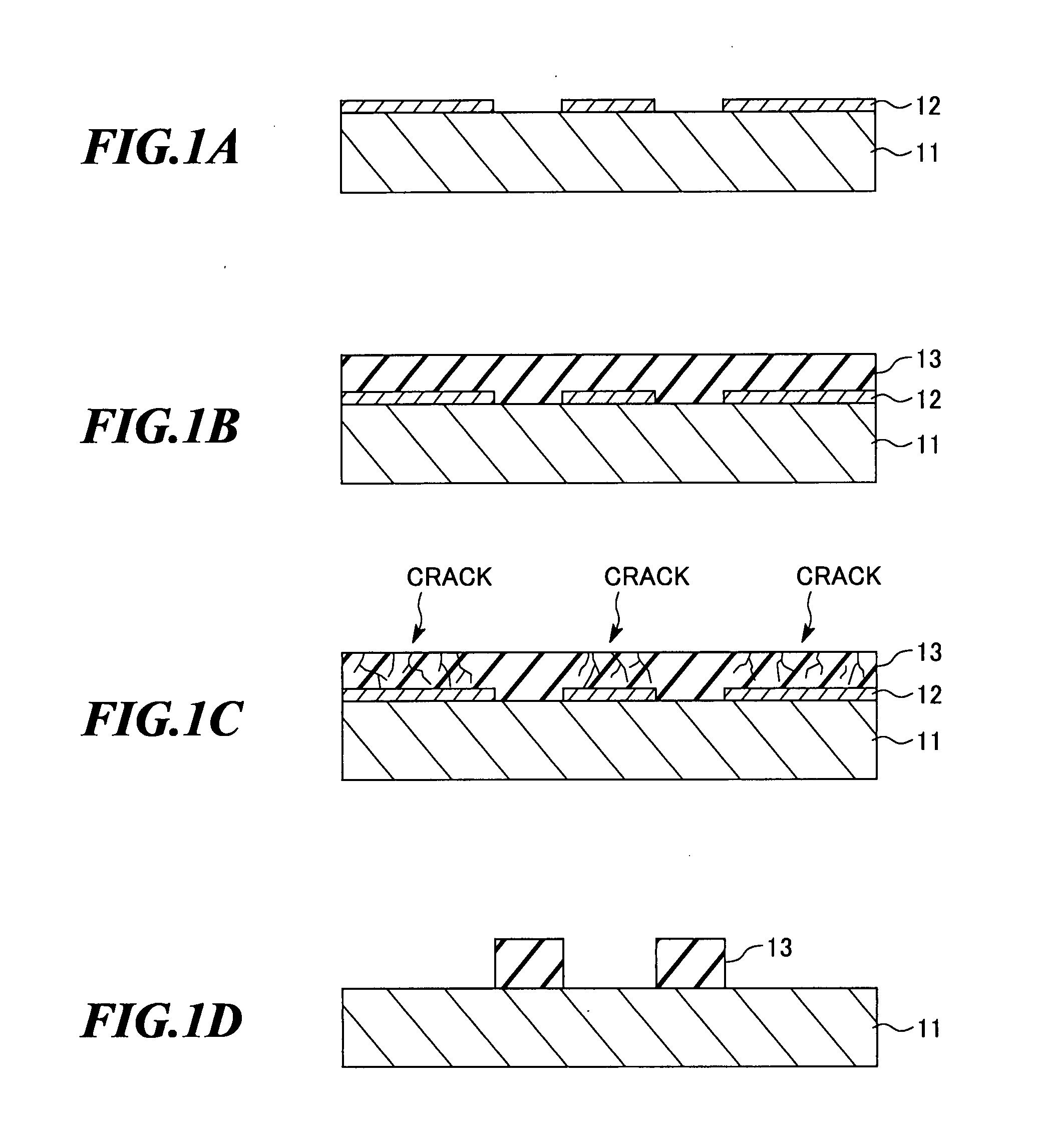
[0021]FIGS. 1A-1D are diagrams for explanation of a method of forming a pattern of an inorganic material film according to the first embodiment of the present invention.

[0022]First, as shown in FIG. 1A, a substrate 11 is prepared, and a pattern of a sacrifice layer 12 is formed thereon. For the substrate 11, a material containing at least one of silicon (Si), copper (Cu)...


PUM


Abstract

A method of forming a pattern of an inorganic material film, which method is more versatile, easy, and practical. The method includes the steps of: (a) forming a sacrifice layer having a pattern on a substrate by employing a material having a different thermal expansion coefficient from that of an inorganic material of the inorganic material film; (b) forming an inorganic material layer on the substrate, on which the sacrifice layer has been formed, at a predetermined deposition temperature by employing the inorganic material; (c) lowering a temperature of at least the inorganic material layer to produce cracks in the inorganic material layer formed on the sacrifice layer; and (d) removing the sacrifice layer and the inorganic material layer formed thereon.

Description

BACKGROUND OF THE INVENTION[0001]1. Field of the Invention[0002]The present invention relates to a method of forming a pattern of an inorganic material film, and specifically, to a method of forming a pattern of an inorganic material film having functionality such as piezoelectric ceramics to be used in micro devices so called micro electrical mechanical systems (MEMS). Further, the present invention relates to a structure containing a pattern of an inorganic material film formed by using such a method.[0003]2. Description of a Related Art[0004]In recent years, research and development of micro electro mechanical systems (MEMS) applying semiconductor manufacturing processes have been increasingly made. Among the systems, the piezoelectric MEMS using a piezoelectric film as a functional film attracts attention as a high-power actuator, and is employed for micropumps, micro-cantilevers, micro ultrasonic transducers, and so on. Here, the functional film refers to a main part (typically...

Claims


Application Information

Patent Timeline
IPC IPC(8): H01L29/84H01L21/00
CPCB81B2201/0271H03H2003/023H03H3/02B81C1/00396
Inventor HISHINUMA, YOSHIKAZUFUJII, TAKAMICHI
Owner FUJIFILM CORP
Why Eureka
Try Eureka