Method of manufacturing semiconductor device

Inactive Publication Date: 2008-03-06
RENESAS TECH CORP
View PDF2 Cites 9 Cited by
  • Summary
  • Abstract
  • Description
  • Claims
  • Application Information

AI Technical Summary

Benefits of technology

[0012] By the present invention, a wire can be cut easily, a suitable-shaped bump

Problems solved by technology

However, since the bump electrode was soft, it became insufficient to crush of a gold wire and was not fully able to thin a gold wire.
Hereby, since the strength of the gold wire became high, the distortion of the gold wire by the reaction at the time of cutting a gold wire, and the peeling from Al pad of a bump electrode had occurred.
That is, there was a problem that a wire could not be cut easily.
There was a problem that the s

Method used


Image

  • Method of manufacturing semiconductor device
  • Method of manufacturing semiconductor device
  • Method of manufacturing semiconductor device

Examples


embodiment 1

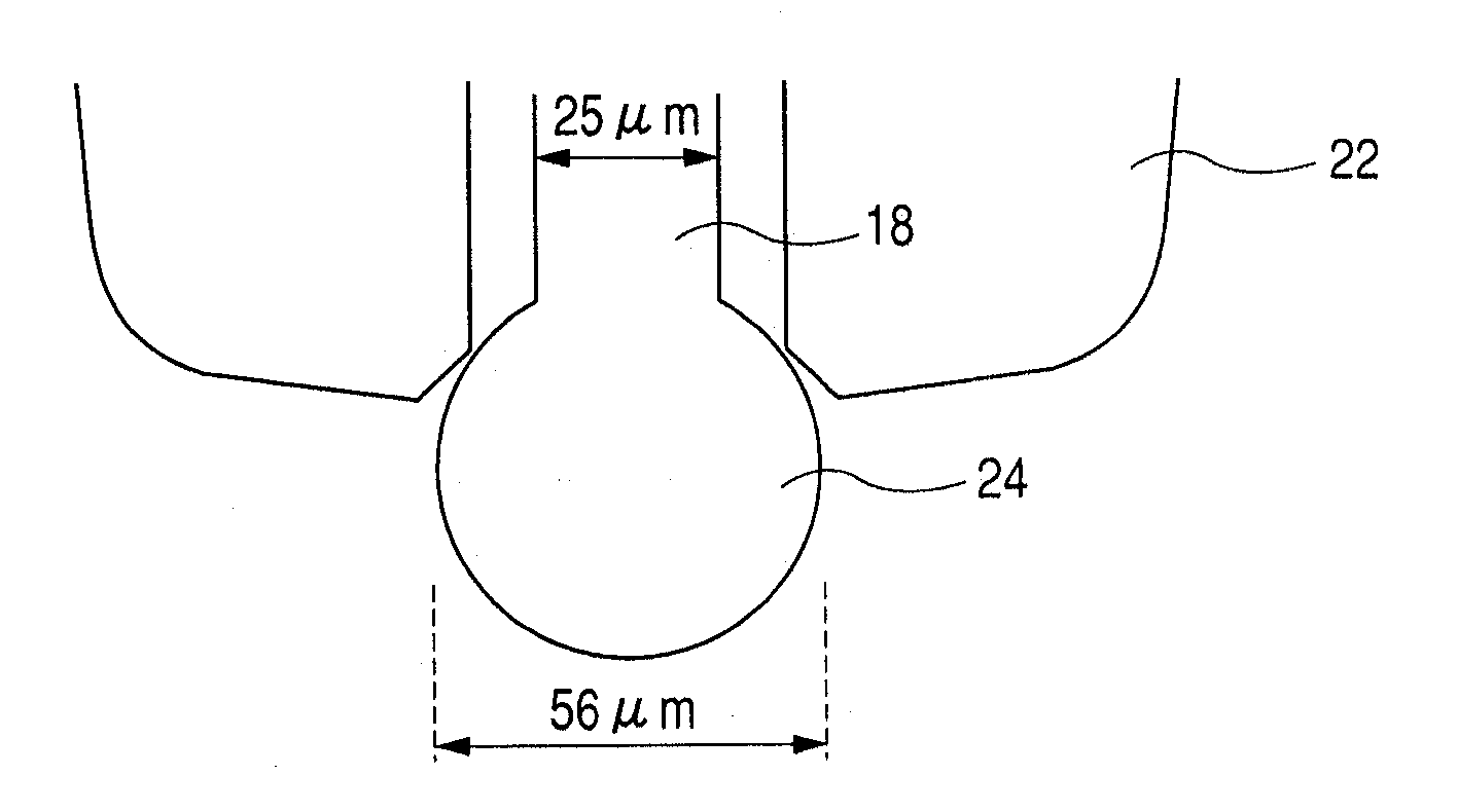
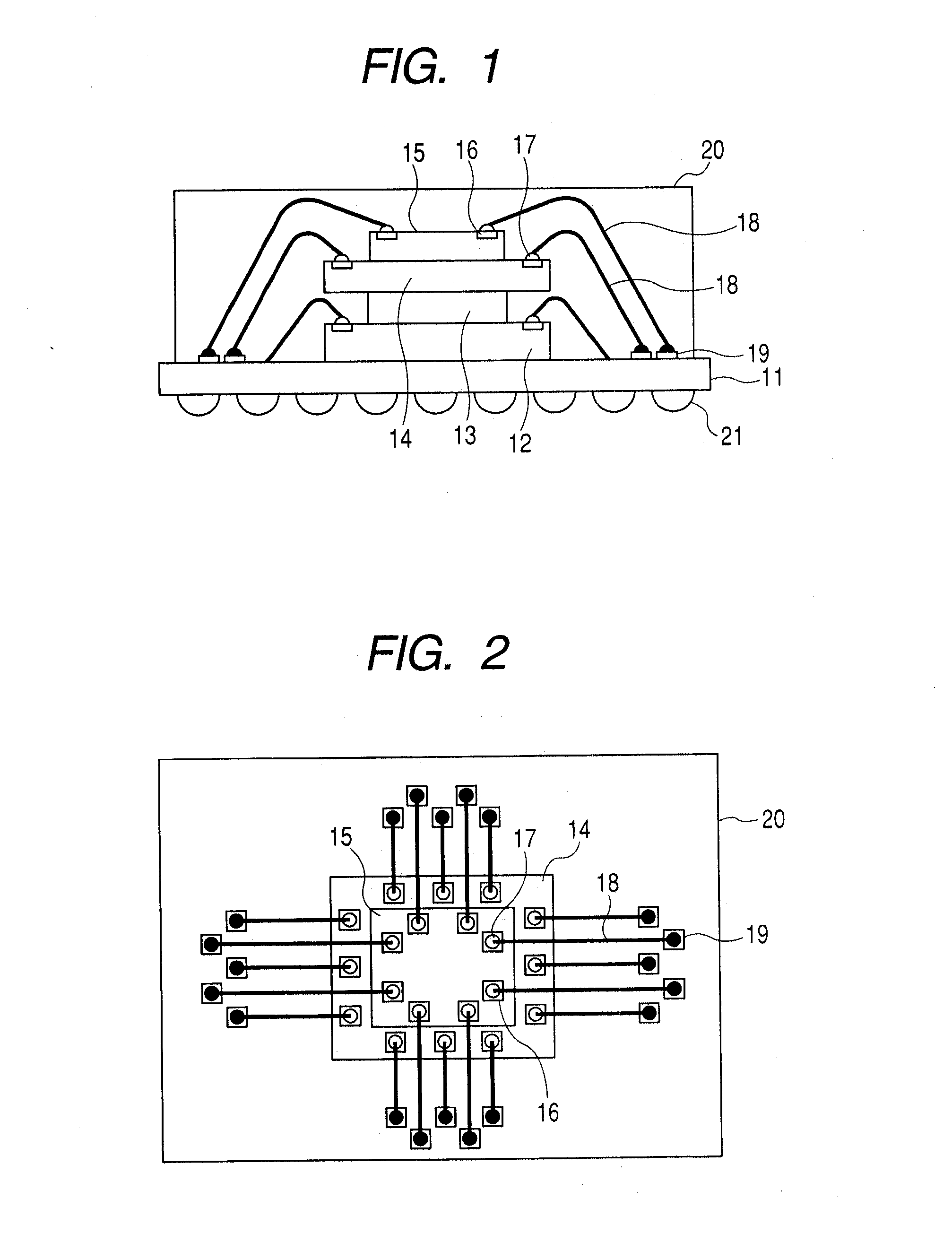
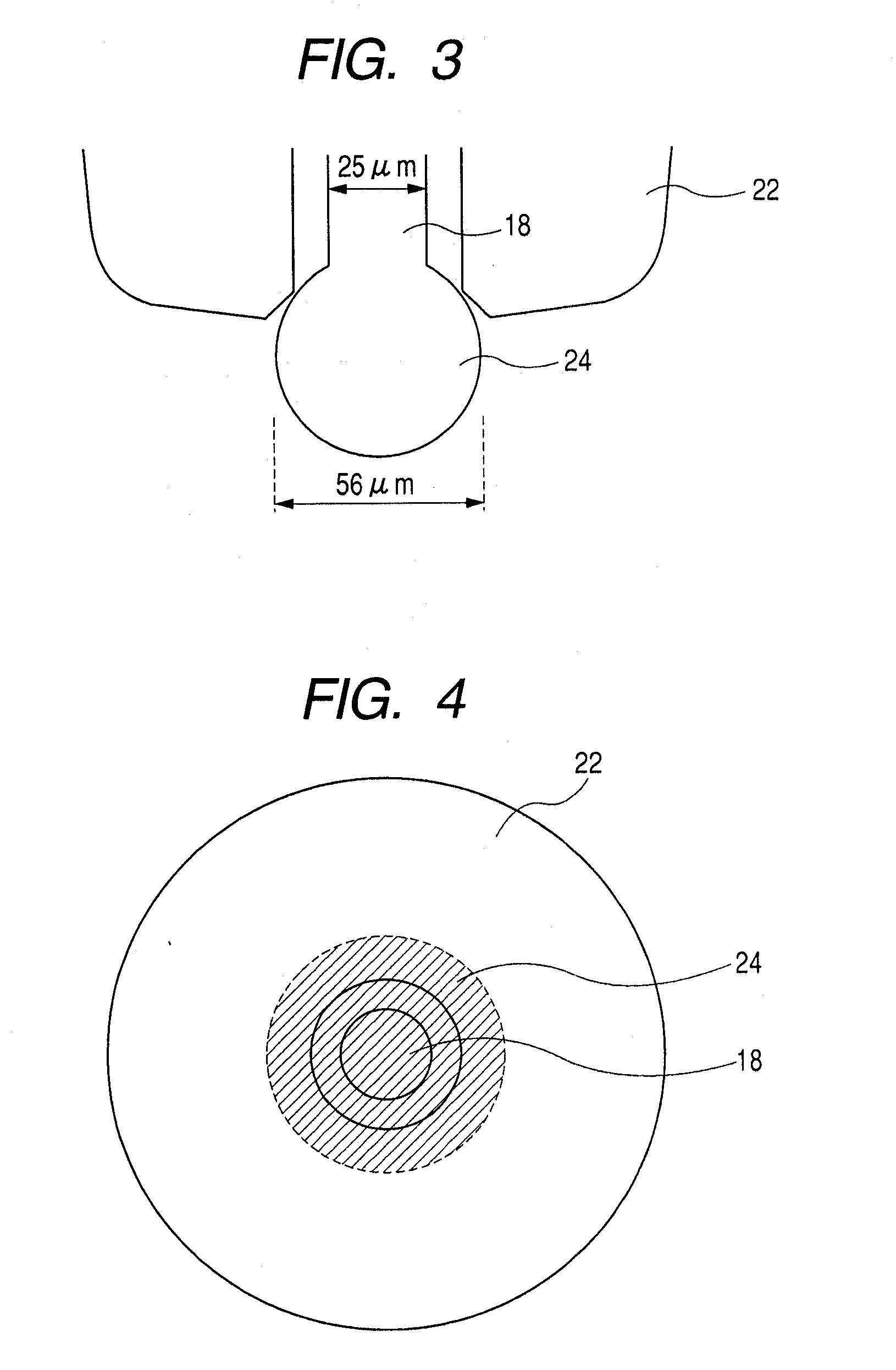
[0026]FIG. 1 is a cross-sectional view showing an example of the semiconductor device manufactured by the manufacturing method concerning Embodiment 1 of the present invention, and FIG. 2 is the top view. On glass epoxy wiring substrate 11, chip 12, spacer chip 13, chip 14, and chip 15 are loaded. Bump electrode 17 is formed on aluminum pad 16 of chips 12, 14, and 15. And ball bonding of the gold wire 18 is done to pad 19, and stitch bonding is done on bump electrode 17. The whole is sealed with sealing resin 20 and solder ball 21 is formed in the bottom of glass epoxy wiring substrate 11.

[0027] Hereafter, the manufacturing method of the semiconductor device concerning Embodiment 1 of the present invention is explained. First, as shown in FIG. 3, gold ball 24 with a larger diameter than gold wire 18 is formed by melting the tip of gold wire 18 which passed to capillary 22 by electric discharge from a torch (un-illustrating). When this state is seen from the upper part, it will beco...

embodiment 2

[0036] Hereafter, the manufacturing method of the semiconductor device concerning Embodiment 2 of the present invention is explained. In this embodiment, as shown in FIG. 17, aluminum pad 16 is formed in a part for the over hang to spacer chip 13 of chip 14. In this case, as shown in FIG. 18, chip 14 bends below according to 30 g of loads of capillary 22 to aluminum pad 16 at the time of formation of bump electrode 17.

[0037] Then, as shown in FIG. 7, after forming bump electrode 17 on aluminum pad 16 and before raising capillary 22, it shall be lower than the time of formation of bump electrode 17, for example, the load of capillary 22 to aluminum pad 16 shall be 5 g or less. And after the tip of capillary 22 has touched bump electrode 17 as it is, it maintains 5 ms or more. As shown in FIG. 17 here, when the length for an over hang of chip 14 is 1.2 mm and the thickness of chip 14 is 90 μm, the length for an over hang of chip 14 is 10 or more times of the thickness of chip 14. In ...


PUM

PropertyMeasurementUnit
Lengthaaaaaaaaaa
Lengthaaaaaaaaaa
Lengthaaaaaaaaaa

Abstract

A manufacturing method of a semiconductor device which can cut a wire easily, can obtain a suitable-shaped bump electrode, and can pull out a wire easily from a capillary is obtained. The method includes the step of forming a bump electrode on a pad with the wire which passed to the capillary after the portion has eaten away in a capillary, a step at which a capillary is raised only 30 μm˜45 μm, a step which dwindles the wire which makes a capillary move only 35 μm˜55 μm to a horizontal direction after raising a capillary, a step which pulls out a wire from the capillary which raises a capillary after dwindling a wire, and the step which cuts a wire by pulling upward on both sides of a wire by a clamper after pulling out a wire from a capillary.

Description

CROSS-REFERENCE TO RELATED APPLICATION [0001] The present application claims priority from Japanese patent application No. 2006-239252 filed on Sep. 4, 2006, the content of which is hereby incorporated by reference into this application. FIELD OF THE INVENTION [0002] The present invention relates to a manufacturing method of a semiconductor device which forms a bump electrode on a pad with the wire which passed to the capillary, and especially relates to a manufacturing method of a semiconductor device which can make the cut of the wire from a bump electrode easy, and can obtain a suitable-shaped bump electrode. DESCRIPTION OF THE BACKGROUND ART [0003] When doing bonding of the gold wire to Al pad on a chip directly, the load of a capillary concentrates and a crack enters into SiO2 interlayer insulation film under Al pad. For this reason, a bump electrode is used for wire bonding of a chip to chip (chip-to-chip). In a thin package, in order to make the height of a gold wire low, rev...

Claims


Application Information

Patent Timeline
IPC IPC(8): B23K1/20B23K31/02
CPCB23K20/005H01L2924/01033B23K2201/40H01L24/45H01L24/48H01L24/78H01L24/80H01L24/85H01L25/50H01L2224/1134H01L2224/13144H01L2224/32145H01L2224/45015H01L2224/45144H01L2224/48091H01L2224/48227H01L2224/48465H01L2224/48471H01L2224/48479H01L2224/48599H01L2224/49175H01L2224/49433H01L2224/78303H01L2224/85045H01L2224/85051H01L2224/85181H01L2224/85186H01L2224/85205H01L2224/85986H01L2225/0651H01L2225/06575H01L2924/01004H01L2924/01013H01L2924/01079H01L2924/014H01L2924/15311B23K20/10H01L2924/01006H01L2924/00013H01L2924/00014H01L2924/20752H01L2224/13099H01L2924/00H01L2924/181H01L2224/05554H01L2224/0557H01L2224/05573H01L2224/05624H01L2224/05571H01L2924/10161H01L24/49H01L2224/0554B23K2101/40H01L2224/78301H01L24/05H01L2224/48137H01L2924/00015H01L2924/00012H01L2224/4554H01L2224/05599H01L2224/0555H01L2224/0556
Inventor ARAKAWA, HIDEYUKI
Owner RENESAS TECH CORP
Why Eureka
Try Eureka