

Method of fabricating display device
a display device and manufacturing method technology, applied in the direction of semiconductor devices, electrical devices, transistors, etc., can solve the problem of increasing the manufacturing cost, and achieve the effect of reducing the number of complicated photolithography steps, reducing waste of materials, and cost reduction
- Summary
- Abstract
- Description
- Claims
- Application Information
AI Technical Summary
Benefits of technology
Problems solved by technology
Method used
Image

Examples
embodiment mode 1
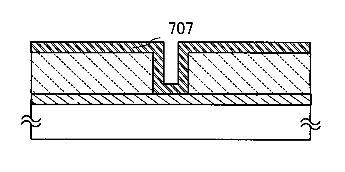
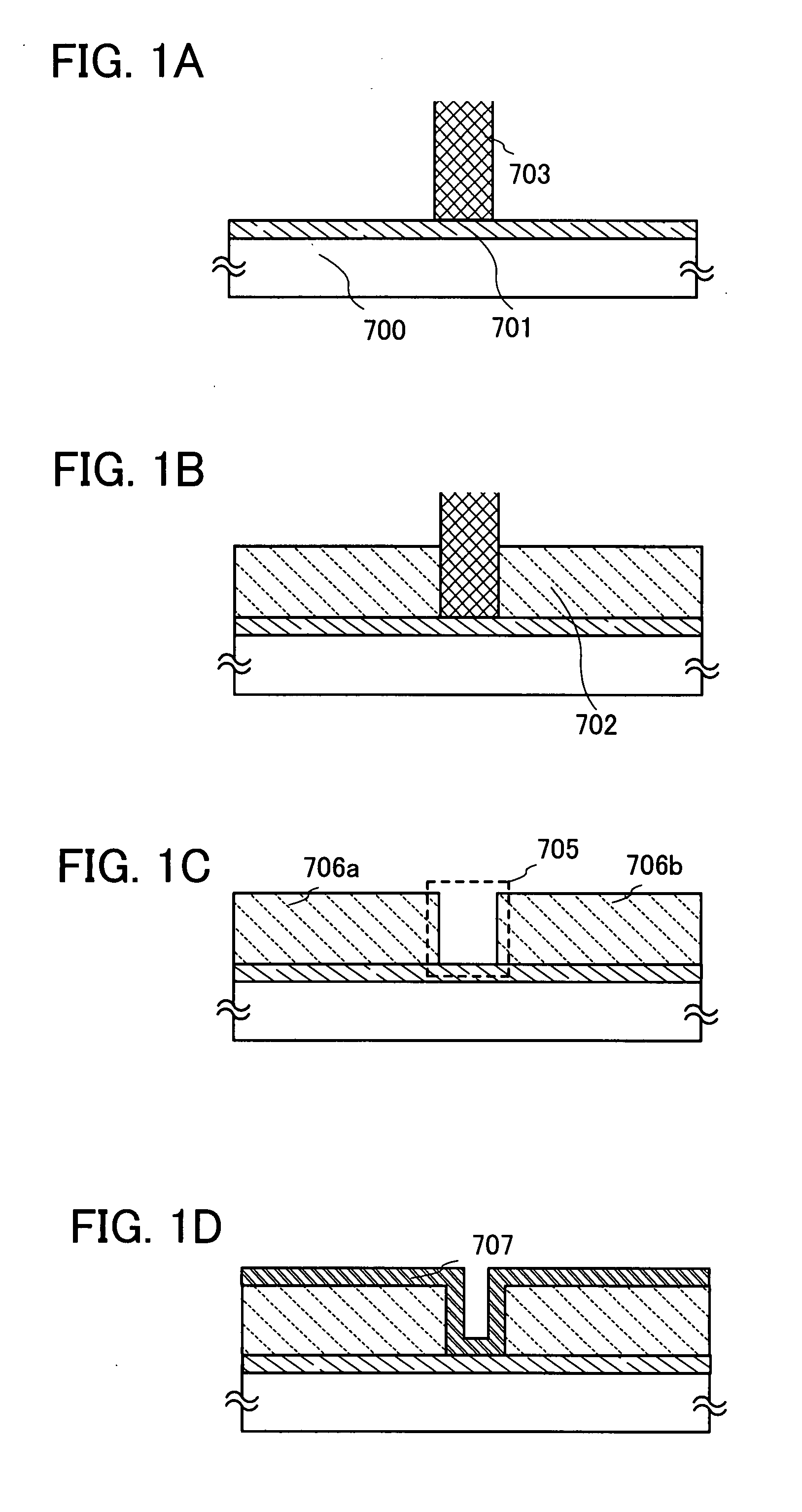
[0057]This embodiment mode will describe a method of forming a contact hole with high reliability at low cost through a simplified process, with reference to FIGS. 1A to 1D.
[0058]In the case of electrically connecting thin films (e.g., a conductive layer and a semiconductor layer) that are stacked with an insulating layer sandwiched therebetween, an opening (so-called contact hole) is formed in the insulating layer. In this case, the insulating layer is selectively formed so as to have an opening without using an etching step. Specifically, a mask is provided in a region where an opening is to be formed, and an insulating layer is formed in a region excluding the mask. After the formation of the insulating layer, the mask is removed physically or chemically, so that an insulating layer having an opening in the region where the mask has been provided is formed. Thus, an insulating layer having an opening is formed over a conductive layer in such a manner that a part of the conductive...
embodiment mode 2
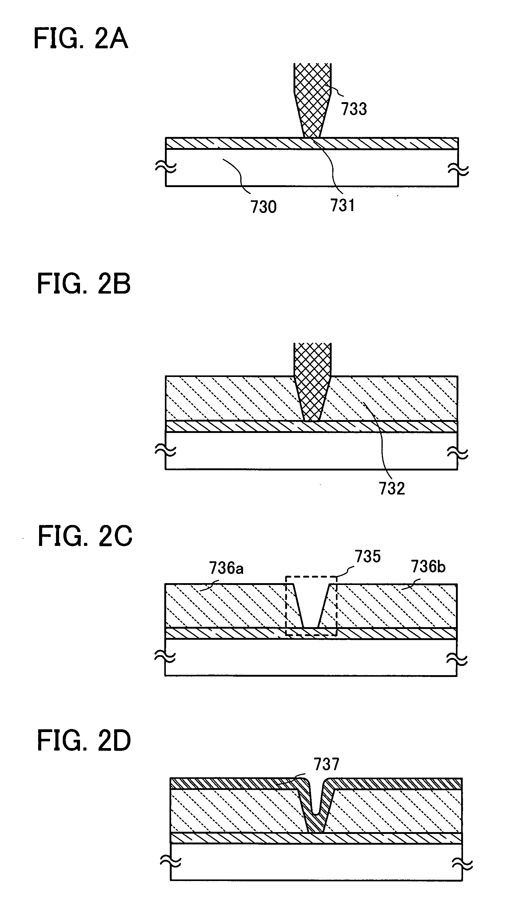
[0091]This embodiment mode will describe a method of forming a plurality of contact holes with high reliability at low cost through a simplified process, with reference to FIGS. 4A to 4H.
[0092]In the case of electrically connecting thin films (e.g., a conductive layer and a semiconductor layer) that are stacked with an insulating layer sandwiched therebetween, an opening (so-called contact hole) is formed in the insulating layer. In this case, the insulating layer is selectively formed so as to have an opening without using an etching step. Specifically, a mask is provided in a region where an opening is to be formed, and an insulating layer is formed in a region excluding the mask. After the formation of the insulating layer, the mask is removed physically or chemically, so that an insulating layer having an opening in the region where the mask has been provided is formed. Thus, an insulating layer having an opening is formed over a conductive layer in such a manner that a part of ...
embodiment mode 3
[0112]This embodiment mode will describe a method of forming a highly reliable display device at low cost through a simplified process, with reference to FIGS. 3A to 3C.
[0113]In this embodiment mode, structures (also referred to as patterns) such as a conductive layer and a semiconductor layer are selectively formed into desired shapes without using a photolithography process. In the invention, structures (also referred to as patterns) include all of component elements of a thin film transistor or a display device that are formed to have predetermined shapes such as conductive layers (e.g., wiring layers, gate electrode layers, source electrode layers, or drain electrode layers), semiconductor layers, mask layers, insulating layers, and the like.
[0114]In this embodiment mode, a light-absorbing film such as a conductive film or a semiconductor film is formed on a first substrate having a light-transmitting property, and then the light-absorbing film is irradiated with laser light fro...
PUM
 Abstract
Description
Claims
Application Information