Nanowire MOSFET with doped epitaxial contacts for source and drain

a technology of epitaxial contacts and nanowires, which is applied in the field of field effect transistors with nanowire channels and doped semiconductor source and drain regions, can solve the problems of loss of catalyst gold, nanowire tapering (in ge nanowires), and difficulty in in-situ dope nanowires during their growth, and achieves no simple methods for aligning contacts and gate to each segmen

Active Publication Date: 2008-03-13
GLOBALFOUNDRIES US INC
View PDF24 Cites 80 Cited by
  • Summary
  • Abstract
  • Description
  • Claims
  • Application Information

AI Technical Summary

Benefits of technology

[0005]The present invention provides a nanowire FET (field effect transistor) with doped source and drain regions. In accordance with the present invention, an undoped nanowire forms the channel region of the inventive FET. Radial epitaxy is used to form the FET source and drain in selected regions of the nanowire.

Problems solved by technology

Forming a doped source and a drain to a semiconductor nanowire presents several challenges.
First, it is difficult to in-situ dope nanowires during their growth since dopants are incorporated into the nanowire body from the gas-phase or by radial growth (E. Tutuc et al., Nano Lett, September 2006, in press).
Third, heavy in-situ doping was shown to lead to nanowire tapering (in Ge nanowires) and loss of gold from the catalyst (in Si nanowires doped with diborane).
Forth, even if segmented doping along a nanowire body can be achieved, there are no simple methods to align the contacts and the gate to each segment.
Fifth, dopant variations will make it hard to control doping in thin nanowires.
This approach has the disadvantage that it can only be used with fat nanowires (diameters larger than 30 nm) since nanowires with small diameters will be amorphized and sputtered by the implant.
Recrystallization of the doped regions may not be possible due to the one-dimensional nature of the nanowire (spontaneous recrystallization will dominate during solid phase epitaxy).

Method used


Image

  • Nanowire MOSFET with doped epitaxial contacts for source and drain
  • Nanowire MOSFET with doped epitaxial contacts for source and drain
  • Nanowire MOSFET with doped epitaxial contacts for source and drain

Examples


example

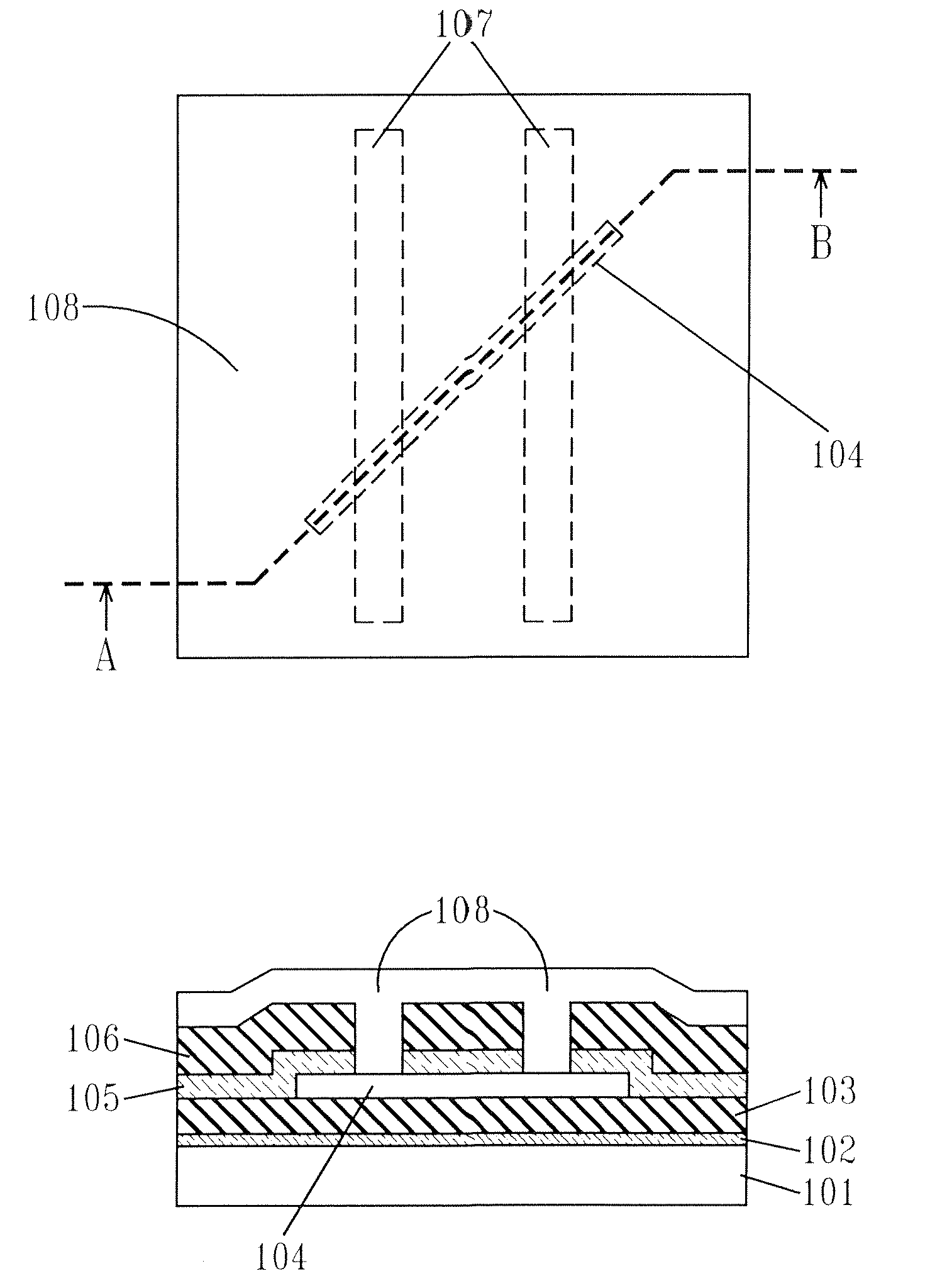
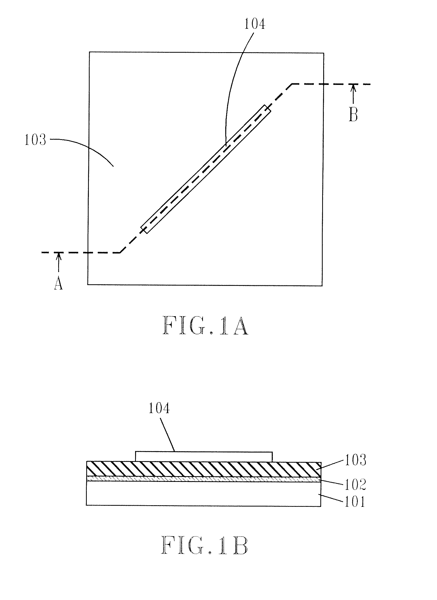
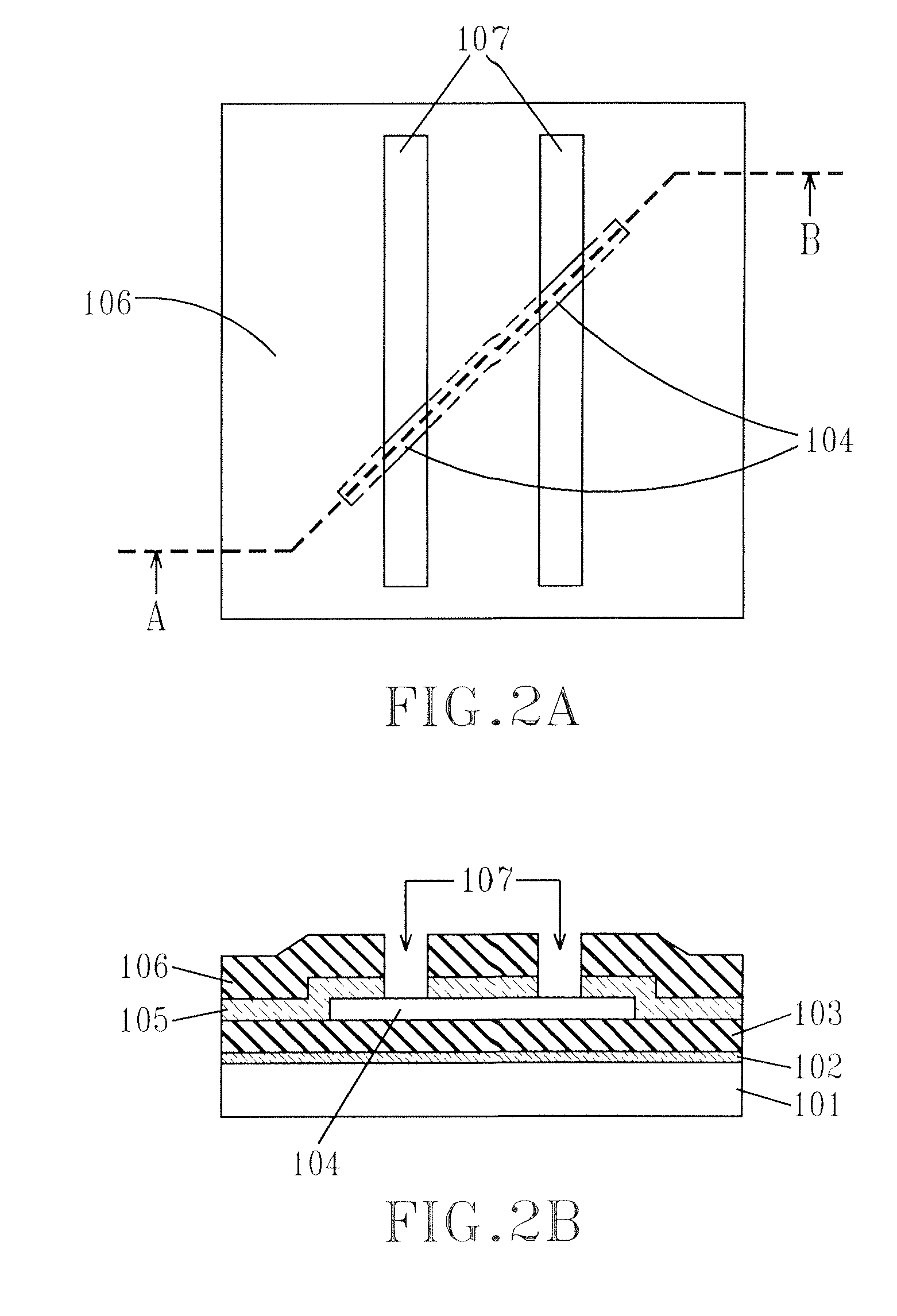
[0039]Using the method discussed in FIGS. 1-4, a silicon nanowire FET with doped silicon source and drain regions was fabricated.

[0040]The nanowires synthesis included the following process steps: A 2 nm thick gold (Au) film was evaporated on a clean silicon (111) substrate. The substrate was then introduced into an UHV-CVD chamber and annealed at 500° C. for 10 minutes. The annealing at 500° C. caused the thin gold film to agglomerate into small gold droplets. These gold droplets were used as the catalyst for the nanowire growth. The substrate temperature was lowered to 420° C., which was the growth temperature. The growth initiated when silane (SiH4) was introduced into the chamber. The silane pressure during growth was held at 2 torr. The growth time was set to grow nanowires that were about 10 microns long. The average nanowire diameter was about 25 nm.

[0041]The gold catalyst was selectively etched in a potassium iodide and iodine (KI / I2) solution. A portion of the substrate (wi...


PUM

PropertyMeasurementUnit
lengthaaaaaaaaaa
diameteraaaaaaaaaa
diameteraaaaaaaaaa

Abstract

A FET structure with a nanowire forming the FET channel, and doped source and drain regions formed by radial epitaxy from the nanowire body is disclosed. A top gated and a bottom gated nanowire FET structures are discussed. The source and drain fabrication can use either selective or non-selective epitaxy.

Description

FIELD OF THE INVENTION[0001]The present invention relates to electronic devices based on semiconductor nanowires, and more specifically to a field effect transistor (FET) with a nanowire channel and doped semiconductor source and drain regions. The present invention also relates to methods of fabricating doped semiconductor source / drain regions which are in contact with the nanowire channel.BACKGROUND OF THE INVENTION[0002]Forming a doped source and a drain to a semiconductor nanowire presents several challenges. First, it is difficult to in-situ dope nanowires during their growth since dopants are incorporated into the nanowire body from the gas-phase or by radial growth (E. Tutuc et al., Nano Lett, September 2006, in press). For example, a lightly doped portion of a nanowire will be counter-doped if a following segment is grown to be heavily doped. Second, due to growth incubation time the onset for a doped region in in-situ doped nanowires will exhibit variations corresponding to...

Claims


Application Information

Patent Timeline
Patent Type & Authority Applications(United States)
IPC IPC(8): H01L29/06
CPCB82Y10/00H01L29/0665H01L29/0673H01L29/458H01L29/78696H01L29/785H01L29/78618H01L29/78684H01L29/7839
Inventor CHU, JACK O.COHEN, GUY M.OTT, JOHN A.ROOKS, MICHAEL J.SOLOMON, PAUL M.
Owner GLOBALFOUNDRIES US INC
Why Eureka
Try Eureka