
Eureka
For R&D, Eureka makes reading and utilizing patents & technical documents easy.
Eureka AIR
Designed for self-driven R&D workflows. Generate viable solutions, solve complex R&D challenges, empower your innovation with AI.

Eureka Materials
Designed for material experts only. Revolutionize your material R&D, from search, analyze, to developing new materials.

TechResearch
Generate reliable direction feasibility study reports for your R&D in just a few steps.

TechSeek
Discover and master advanced knowledge NOW. Basics, ideas, possibilities, all at once.

TechMind
As an expert in R&D Theories, TechMind can generates customized viable solutions instantly.

TechRisk
Analyze your overall solution with one click, know your potential R&D risks in advance.

TechMonitor
Get weekly tech updates, stay abreast of the latest tech innovations and key insights.
Semiconductor memory device and method of fabricating semiconductor memory device
- Summary
- Abstract
- Description
- Claims
- Application Information
AI Technical Summary
Problems solved by technology
Method used
Image

Examples
first embodiment
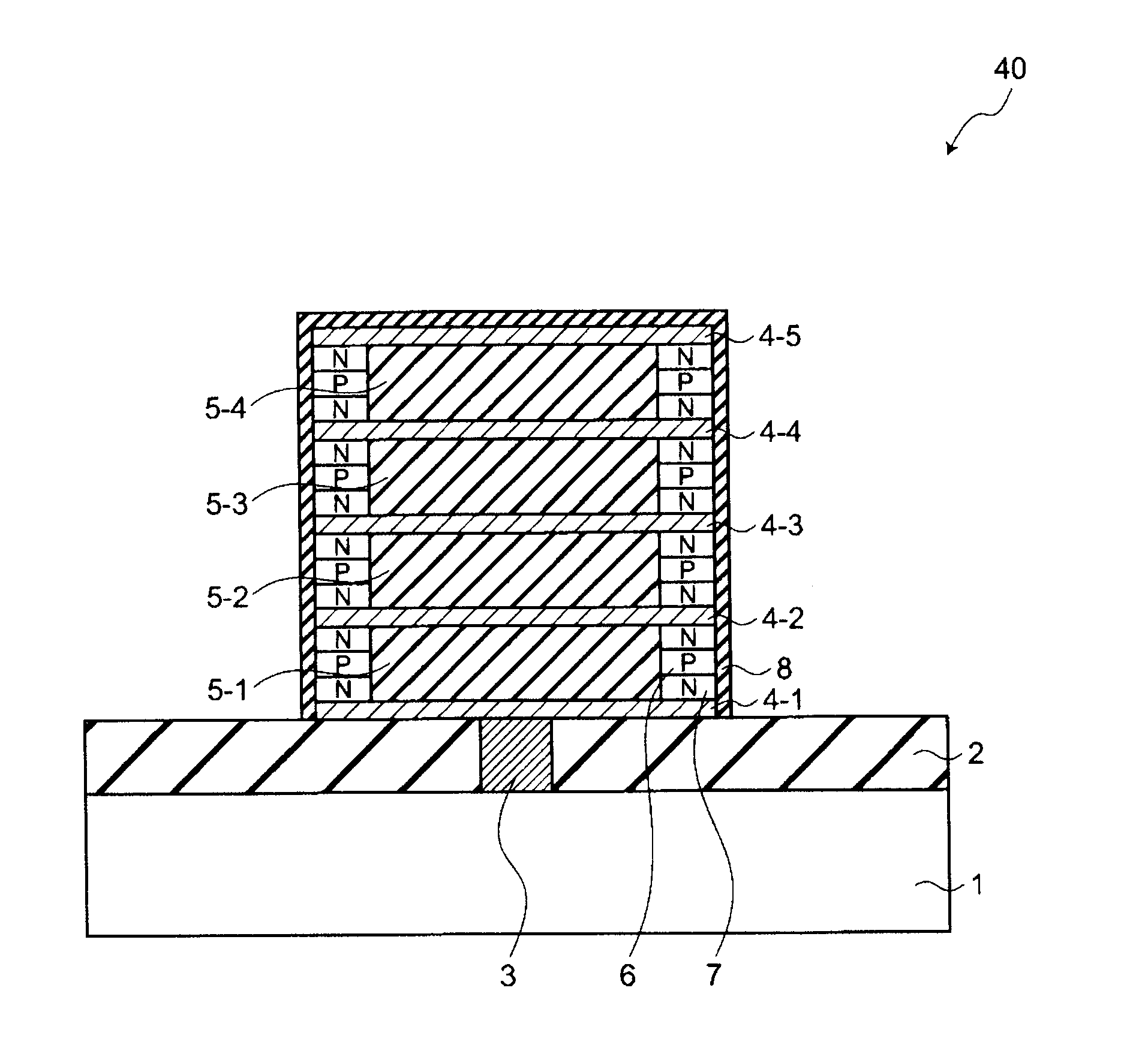
[0024]First, a semiconductor memory device and a fabricating method of the semiconductor memory device according to a first embodiment of the present invention will be described below in detail with reference to the drawing mentioned above.
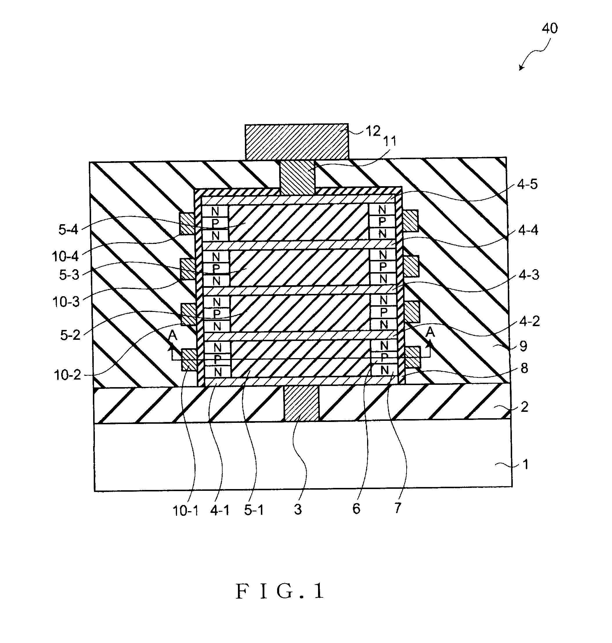
[0025]FIG. 1 is a schematic cross-sectional view showing a ferroelectric memory including a memory cell portion in a first embodiment of the present invention. FIG. 2 is a schematic plane view along line A-A in FIG. 1 showing the ferroelectric memory including the memory cell portion in the first embodiment of the present invention. FIG. 3 is an equivalent circuit diagram showing the ferroelectric memory including the memory cell portion in the first embodiment of the present invention.
[0026]The ferroelectric capacitor and the memory cell are formed over a semiconductor substrate in layer in the first embodiment.
[0027]As shown in FIG. 1, a ferroelectric memory 40 is a Chain FeRAM (Ferroelectric Random Access Memory) as a ferroelectric memory. The ...
second embodiment
[0063]Next, a semiconductor memory device and the fabricating method of the semiconductor memory device according to a second embodiment of the present invention will be described below in detail with reference to the drawing mentioned above. FIG. 10 is a schematic cross-sectional view showing a ferroelectric memory including a memory cell portion in the second embodiment of the present invention. In the second embodiment, a substrate formation method of a memory cell transistor in a Chain FeRAM as a ferroelectric memory is changed as compared with the substrate formation method in the first embodiment.
[0064]It is be noted that the same or similar reference numerals are applied to the same or similar parts and elements throughout the drawings, and the description of the same or similar parts and elements will be omitted or simplified.
[0065]As shown in FIG. 10, a ferroelectric memory 40a is a Chain FeRAM as a ferroelectric memory. The ferroelectricmemory 40a having a plurality of cyl...
third embodiment
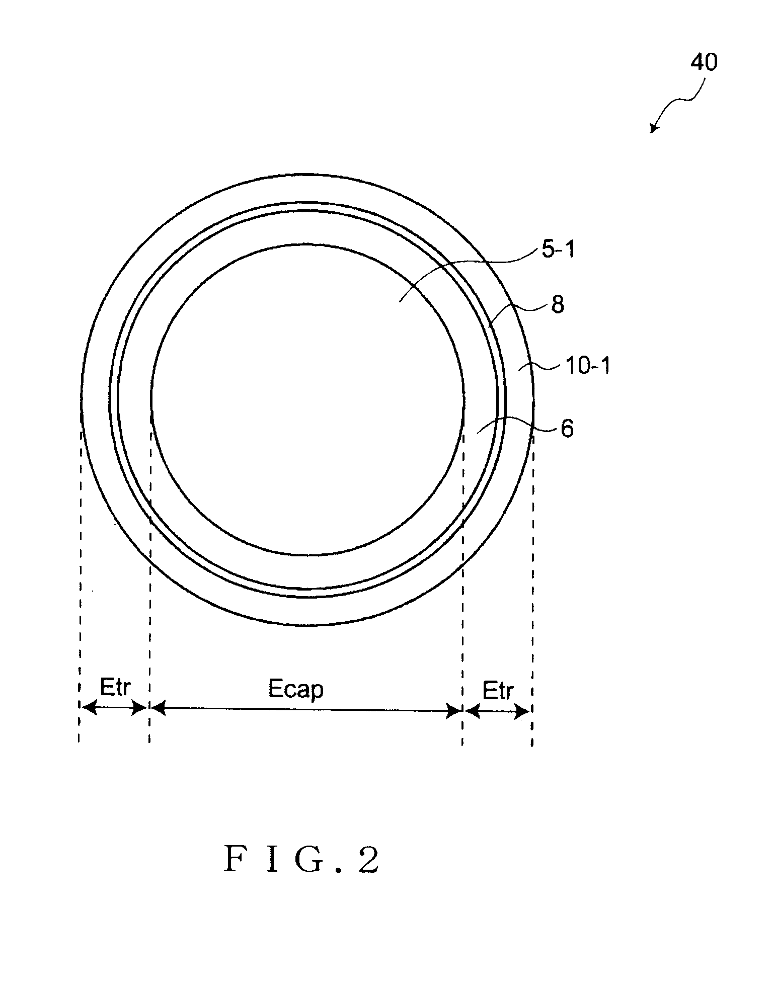
[0085]Next, a semiconductor memory device according to a third embodiment of the present invention will be described below in detail with reference to the drawing mentioned above. FIG. 14 is a schematic plane view showing a ferroelectric memory including a memory cell portion in the third embodiment of the present invention. In this embodiment, a feature of a memory cell portion in a Chain FeRAM as a ferroelectric memory is changed as compared with the feature of the memory cell portion in the first embodiment.
[0086]It is be noted that the same or similar reference numerals are applied to the same or similar parts and elements throughout the drawings, and the description of the same or similar parts and elements will be omitted or simplified.
[0087]As shown in FIG. 14, a memory cell portion of a ferroelectric memory 40b has a square prism type. The center of the memory cell portion with the square prism type is a capacitor region Ecap composed of the ferroelectric film 5. A periphera...
PUM
 Abstract
Description
Claims
Application Information
 - R&D Engineer
- R&D Manager
- IP Professional
- Industry Leading Data Capabilities
- Powerful AI technology
- Patent DNA Extraction
Browse by: Latest US Patents, China's latest patents, Technical Efficacy Thesaurus, Application Domain, Technology Topic, Popular Technical Reports.
© 2024 PatSnap. All rights reserved.Legal|Privacy policy|Modern Slavery Act Transparency Statement|Sitemap|About US| Contact US: help@patsnap.com