Lateral high-voltage devices with optimum variation lateral flux by using field plate

a technology of lateral flux and high-voltage devices, which is applied in the direction of semiconductor devices, semiconductor/solid-state device details, electrical apparatus, etc., can solve the problems of low permittivity and few doses, and achieve the effect of eliminating such charges

Inactive Publication Date: 2008-03-20
UNIV OF ELECTRONICS SCI & TECH OF CHINA
View PDF3 Cites 12 Cited by
  • Summary
  • Abstract
  • Description
  • Claims
  • Application Information

AI Technical Summary

Benefits of technology

[0013]There are some possible reasons to make a floating field plate being charged. For instance, after the insulating layers have absorbed irradiation, or after some local areas have suffered to having high electric field and being breakdown. In order to eliminate such charges, one method is to connect each floating field plate to a certain floating field limiting ring. Then, when the device is turned-on with the voltage across the voltage-sustaning region being very low or when the device has not been applied any voltage, the potentials of all field plates are close to the potential of the substrate and the charges on the field plates can be released.
[0014]With the surface voltage-sustaining region using floating field plates, not only low-side high voltage lateral devices can be made, but also high-side high voltage lateral devices can be made.

Problems solved by technology

However, most popular technologies of integrated circuits are CMOS and BiCMOS technologies, and in such technologies, few can provide the necessary doses as well as depths of n-type and p-type impurities required according to Ref.
Not to mention, almost no technology in integrated circuits contain a process to fabricate a material of a permittivity much higher than that of the semiconductor as required in Ref.

Method used


Image

  • Lateral high-voltage devices with optimum variation lateral flux by using field plate
  • Lateral high-voltage devices with optimum variation lateral flux by using field plate
  • Lateral high-voltage devices with optimum variation lateral flux by using field plate

Examples


Embodiment Construction

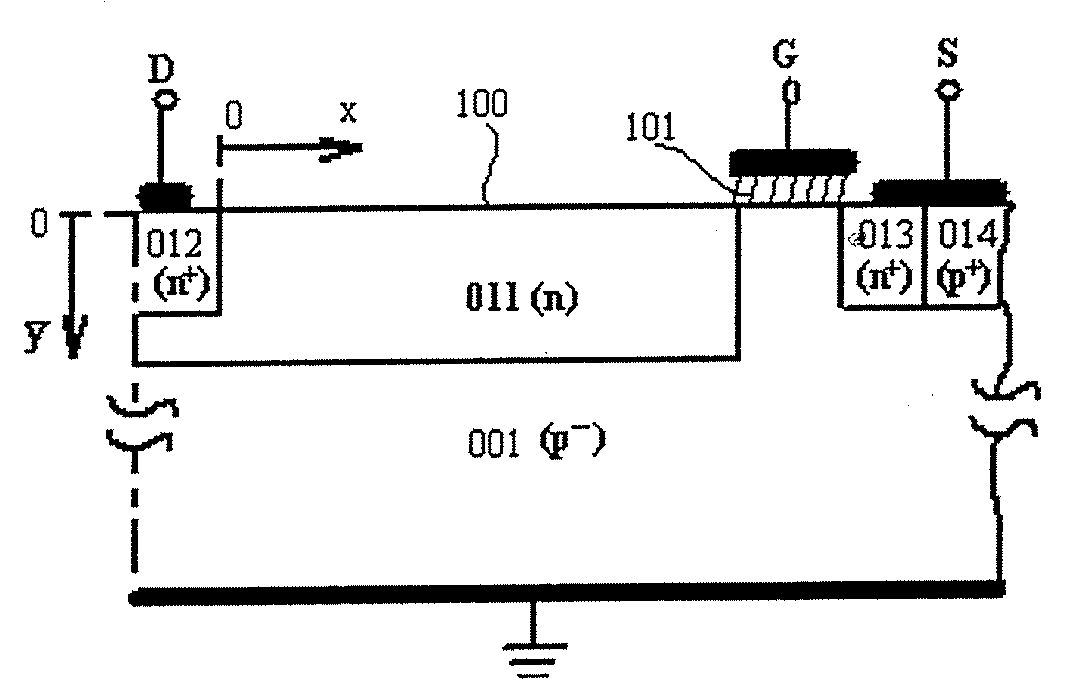
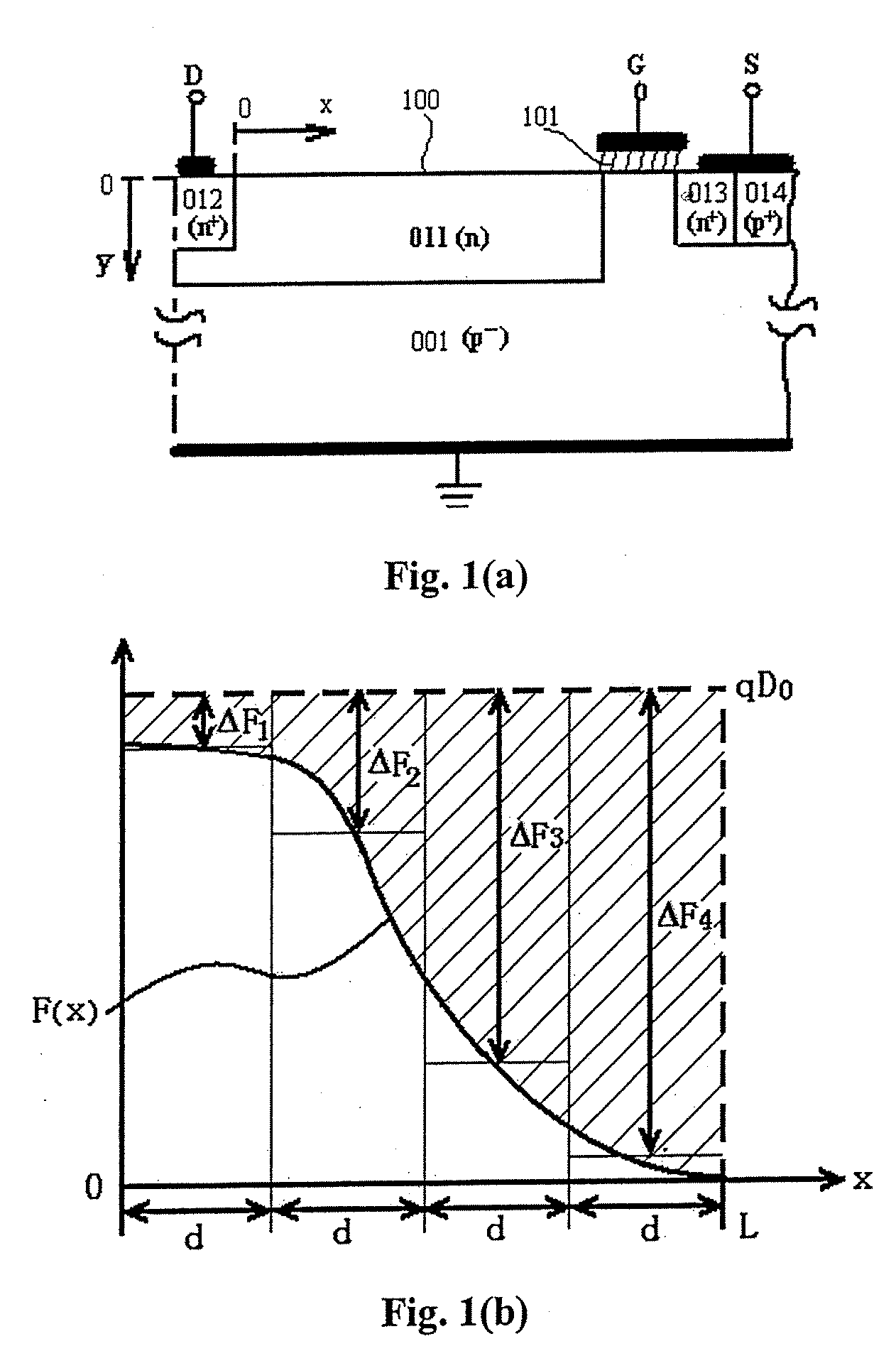
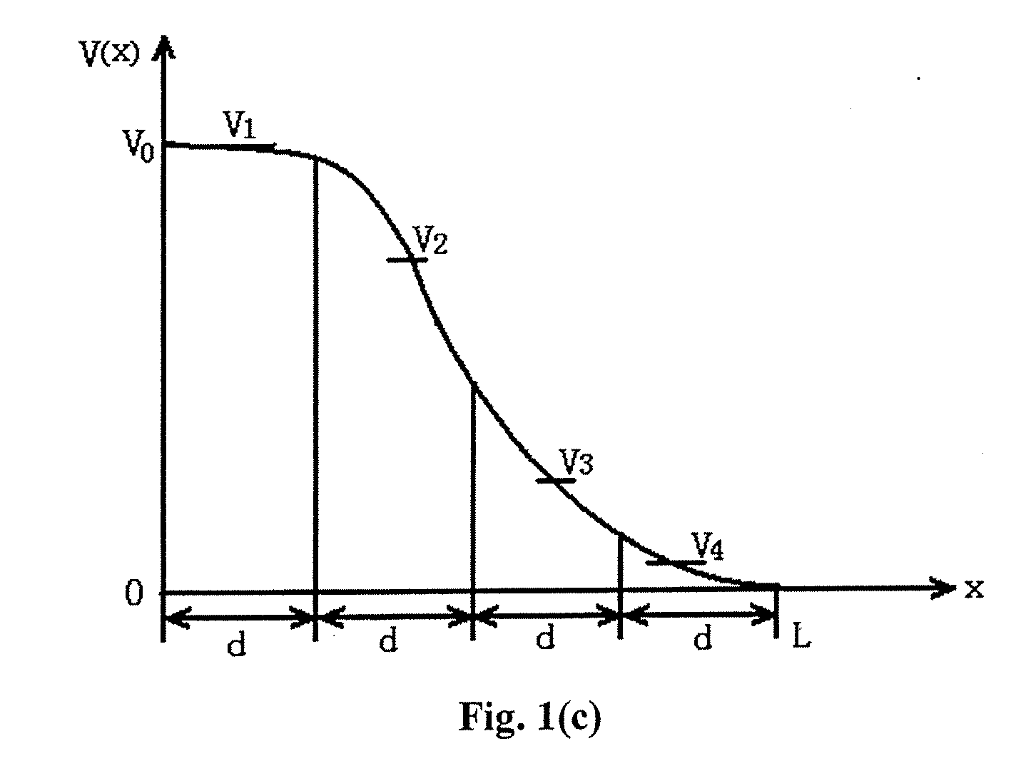
[0052]FIG. 1(a) shows schematically the structure of a lateral MOST, where p−-region 001 is the substrate, n-region 011 is the surface voltage-sustaining region, also called drift region, D, S and G stand for drain, source and gate electrodes respectively. The shaded area 101 is the gate oxide layer or the gate insulator layer. D is connected to n+-drain region 012, S is connected to n+-source region 013 which is connected to p+-source contact region 014 and thus connected to p−-substrate region 001. According to Ref. [1] and [2], in the ideal case, the electric flux density produced by the n-type voltage-sustaining region is F(x) shown as solid line in FIG. 1(b), where the x-axis is shown in FIG. 1(a). F(x) has its maximum value, about 2εsVB / Wpp, at the place x=0, where εs is the permittivity of the semiconductor, VB is the breakdown voltage and Wpp is the thickness of the depletion layer of a one-sided abrupt parallel-plane junction with the same substrate under the breakdown volt...


PUM


Abstract

A semiconductor lateral voltage-sustaining region and devices based thereupon. The voltage-sustaining region is made by using the Metal-Insulator-Semiconductor capacitance formed by terrace field plate to emit or to absorb electric flux on the semiconductor surface, so that the effective electric flux density emitted from the semiconductor surface to the substrate approaches approximately the optimum distribution, and a highest breakdown voltage can be achieved within a smallest distance on the surface. The field plates can be either floating ones, or connected to floating field limiting rings. Coupling capacitance between different plates can also be used to change the flux distribution.

Description

FIELD OF THE INVENTION [0001]The present invention relates to semiconductor devices. More specifically, the present invention relates to the surface voltage-sustaining region, i.e., the drift region of lateral high-voltage devices. The present invention also relates to edge termination techniques of semiconductor high-voltage vertical devices.BACKGROUND OF THE INVENTION [0002]It has been pointed out in Ref. [1, 2], that one can use optimum variation lateral doping, shortly as VLD, to achieve highest breakdown voltage within a minimum distance on the surface. The breakdown voltage reached by using such method is close to the breakdown voltage of a one-sided abrupt parallel plane junction made by the same substrate. Furthermore, the methods of implementation of high-side devices as well as low-side devices by using optimum VLD were proposed in references [4, 5].[0003]It has been proposed in Ref. [3] that the idea of optimum VLD, in its substantial physical mechanism, should be changed...

Claims


Application Information

Patent Timeline
Patent Type & Authority Applications(United States)
IPC IPC(8): H01L23/58
CPCH01L23/585H01L27/088H01L29/0619H01L29/0692H01L29/1095H01L29/402H01L29/404H01L2924/0002H01L29/7816H01L29/7824H01L29/7835H01L29/8611H01L2924/00
Inventor CHEN, XINGBI
Owner UNIV OF ELECTRONICS SCI & TECH OF CHINA
Why Eureka
Try Eureka