
Multi-layer ceramic capacitor and manufacturing method thereof

a multi-layer ceramic capacitor and manufacturing method technology, applied in the direction of variable capacitors, fixed capacitor details, fixed capacitors, etc., can solve the problems of lowering the reliability of multi-layer ceramic capacitors, lowering the life time property, and varying thickness of internal electrodes, so as to achieve high reliability, good life time property, and high insulating property

Inactive Publication Date: 2008-03-20
TAIYO YUDEN KK
View PDF7 Cites 11 Cited by
  • Summary
  • Abstract
  • Description
  • Claims
  • Application Information

AI Technical Summary

Benefits of technology

[0010]In an embodiment, the present invention is intended to overcome at least one of the foregoing problems and provide a multi-layer ceramic capacitor of a high reliability having a high insulating property and a good life time property even when the lamellation proceeds for the dielectric ceramics, and a method of manufacturing such a multi-layer ceramic capacitor.
[0013]According to the first embodiment of the invention, since the grain number per one layer can be increased than usual, the boundary number can be ensured sufficiently to improve the life time property. Further, since the grain growth can be suppressed to decrease the unevenness formed on the boundaries between the dielectric ceramics and the internal electrodes, variation in the thickness of the internal electrodes can be decreased even when the internal electrodes are lamellated, thereby decreasing the portion where the strength of the electric field increases locally. Accordingly, the reliability of the multi-layer ceramic capacitor can be improved.
[0014]Further, in a second embodiment of the invention, there is provided a multi-layer ceramic capacitor wherein the average value for the particle diameter of the raw material powder of the perovskite dielectric substance as the raw material for the dielectric material ceramics is from 30 to 100 nm. According to the second embodiment of the invention, since the sintering reactivity of the raw material powder is increased, grain boundaries having high resistance can be formed even with less grain growth to improve the insulating property.
[0015]Further, the invention provides, in a further embodiment, a method of manufacturing a multi-layer ceramic capacitor having dielectric ceramics formed of a raw material powder of a perovskite dielectric substance and an additive as an extraneous material, which includes using a raw material powder with an average value for the grain diameter of from 30 to 100 nm as the raw material powder of the perovskite dielectric substance and forming dielectric ceramics having grains undergoing grain growth to 1.2 to 1.5 times the average value for the grain diameter of the raw material powder. According to this manufacturing method, it is possible to obtain a multi-layer ceramic capacitor of a high reliability having a high insulating property and a good life time property even when the dielectric ceramics are lamellated.
[0016]According to embodiments of the invention, a multi-layer ceramic capacitor of a high reliability having a high insulating property even under a high electric field and a good life time property can be obtained.

Problems solved by technology

Accordingly, this resulted in a problem of lowering the reliability of the multi-layer ceramic capacitor.
However, since such raw material powder is highly reactive and grain growth tends to proceed, this resulted in a problem that the grains were grown to those having an average value for the diameter of 0.15 μm or more in the existent manufacturing process for the dielectric ceramics.
Further, while the lamellation proceeds also for the internal electrodes along with lamellation of the dielectric ceramics, as the lamellation proceeds in the internal electrodes, thickness of the internal electrode varies due to the unevenness caused to the boundary between the dielectric ceramics and the internal electrodes.
Accordingly, this resulted in a problem of increasing the number of portions where the strength of the electric field increases locally to lower the life time property.

Method used


Image

  • Multi-layer ceramic capacitor and manufacturing method thereof
  • Multi-layer ceramic capacitor and manufacturing method thereof

Examples


Embodiment Construction

[0021]The present invention will be explained in detail with reference to preferred embodiments. However, the preferred embodiments are not intended to limit the present invention.

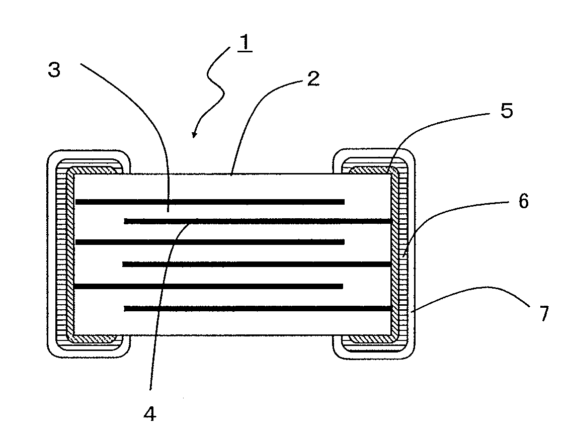
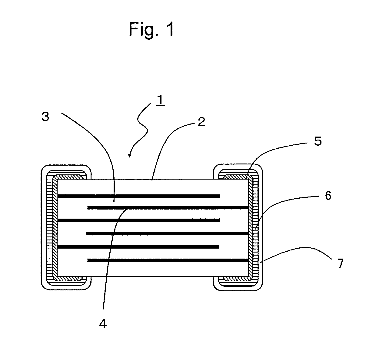
[0022]A preferred embodiment of a multi-layer ceramic capacitor according to the invention is to be described. A multi-layer ceramic capacitor 1 of this embodiment has, as shown in FIG. 1, multi-layer ceramics 2 comprising a dielectric ceramic layer 3 and internal electrodes 4 formed so as to oppose to each other by way of the dielectric ceramic layer 3 and so as to be led out to different end faces alternately. End termination electrodes 5 are formed on both end faces of the multi-layer ceramics 2 so as to be connected electrically with the internal electrodes and a first plating layer 6 and a second plating layer 7 are optionally formed thereon.

[0023]The dielectric ceramics 3 have grains comprising, as a main ingredient, a perovskite dielectric substance represented by ABO3 (in which A represents one or ...


PUM

PropertyMeasurementUnit
diameteraaaaaaaaaa
particle diameteraaaaaaaaaa
grain diameteraaaaaaaaaa

Abstract

A multi-layer ceramic capacitor has substantially hexagonal shape multi-layer ceramics, internal electrodes formed so as to oppose to each other by way of the dielectric ceramics and led to different end faces alternately in the multi-layer ceramic body, and end termination electrodes formed on both end faces of the multi-layer ceramics and electrically connected to the internal electrodes respectively led out to the end faces, in which the ratio between the average value D for the diameter of the grains and the average value d for the particle diameter of the raw material powder of the perovskite dielectric substance is: 1.2≦D / d≦1.5, and the average value D for the diameter of the grains constituting the dielectric ceramics is from 40 to 150 nm.

Description

BACKGROUND OF THE INVENTION[0001]1. Field of the Invention[0002]The present invention provides a method of providing a multi-layer ceramic capacitor of high reliability having a high insulating property even under a high electric field and a good life time property, and a manufacturing method thereof.[0003]2. Description of the Related Art[0004]A multi-layer ceramic capacitor has multi-layer ceramics constituted with dielectric ceramics formed of a perovskite raw material powder represented by ABO3 (in which A represents one or more member selected from Ba, Ca, and Sr, and B represents one or member selected from Ti and Zr) and an additive, internal electrodes formed in the multi-layer ceramics so as to oppose to each other by way of the dielectric ceramics and led out to different end faces alternately, and end termination electrodes formed on both end faces of the multi-layer ceramics and electrically connected to the internal electrodes respectively.[0005]As the dielectric materi...

Claims


Application Information

Patent Timeline
Patent Type & Authority Applications(United States)
IPC IPC(8): H01G4/06H01G7/00
CPCB82Y30/00C04B35/4682C04B2235/3206C04B2235/3224C04B2235/3265C04B2235/3418Y10T29/435C04B2235/5454C04B2235/656C04B2235/781C04B2235/785H01G4/1227H01G4/30C04B2235/5445
Inventor TANIGUCHI, KATSUYAMIZUNO, YOUICHI
Owner TAIYO YUDEN KK
Learn More