

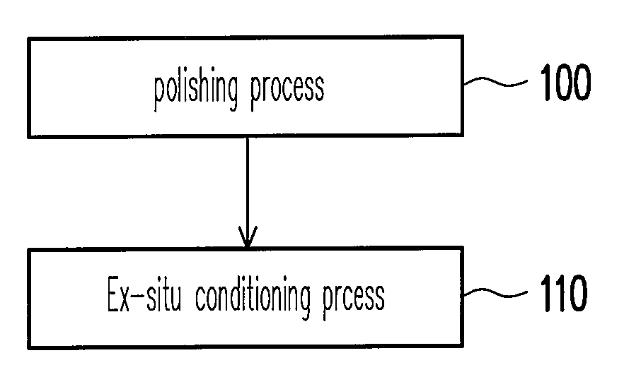
Chemical mechanical polishing process
- Summary
- Abstract
- Description
- Claims
- Application Information
AI Technical Summary
Benefits of technology
Problems solved by technology
Method used
Image

Examples
embodiment 1
[0036]FIG. 3 is a drawing, schematically illustrating the polishing timing of the CMP process of the present invention in comparing with a convention CMP process, according to a first embodiment of the invention.
[0037]Referring to FIG. 3, when the CMP apparatus has three polishing regions, indicated by P1, P2 and P3 as the first polishing platen, the second polishing platen, and the third polishing platen in the polishing regions. Each polishing region has a polishing time period by 60 seconds. In addition, a transferring time for the wafer being moved to the next polishing region, equivalent to the rotation time of the mechanical arm, is set to 6 seconds. The polishing platens P1 and P2 have the ex-situ conditioning time by 20 seconds while the polishing platen P3 does not have the ex-situ conditioning.
[0038]As known from FIG. 3, when the polishing step at P1 finishes (at time point 0 of the time coordinate of FIG. 3), in the embodiment of the invention, the ex-situ conditioning st...
embodiment 2
[0039]FIG. 4 is a drawing, schematically illustrating the polishing timing of the CMP process of the present invention in comparing with a convention CMP process, according to a second embodiment of the invention.
[0040]The difference of embodiment 2 from embodiment 1 is that the polishing time for P1 and P2 is set to 60 second while the P3 is set to 70 seconds. When the polishing step for the first wafer at P1 has finished, at time point 0 of the time coordinate, the ex-situ conditioning step and the transferring step are performed at the same time. After the first wafer, being moved to P2, is polished by 14 second, at time point 20 of the time coordinate, P1 has finished the ex-situ conditioning step and performed the polishing step for the second wafer. In addition, when the first wafer being moved to P2 finishes the polishing step, at time point 80 of time coordinate. After waiting for 14 seconds, the first wafer and the second wafer can be simultaneously transferred to P3 for po...
PUM
 Abstract
Description
Claims
Application Information