Directional coupler and RF circuit module

a circuit module and directional coupler technology, applied in the direction of pulse generators, waveguides, pulse techniques, etc., can solve the problems of increased loss on the main line side, and achieve the effect of efficient generation of magnetic fields, and increased coupling per unit area

Inactive Publication Date: 2008-03-20
RENESAS ELECTRONICS CORP
View PDF15 Cites 54 Cited by
  • Summary
  • Abstract
  • Description
  • Claims
  • Application Information

AI Technical Summary

Benefits of technology

[0019]A directional coupler of the present invention is a directional coupler comprising a main-line, a sub-line, and a ground plane and is characterized by that the main-line and / or the sub-line form at least one winding of a loop and the loop is disposed so that a main component of a vector vertically penetrating the loop is horizontal with respect to the ground plane. By disposing the loop so that the main component of a vector vertically penetrating the loop is horizontal with respect to the ground plane, a magnetic field can be generated efficiently from the main-line and / or the sub-line, the coupling per unit area is increased, and the downsizing is achieved.
[0020]Here, if a first section in which the main-line and / or the sub-line run in parallel in a direction of the same electric current flowing in the main-line and / or the sub-line in maximum times in the loop is disposed at a position separated from the ground plane by a distance longer than that of the other section, that is, a second section, and a portion of the main-line and a potion of the sub-line contributing to a coupling between the main-line and the sub-line are disposed at a position separated from the ground plane by a distance approximately equal to or longer than that of the first section, the portion where a magnetic field is generated most strongly is separated from the ground plane by the longest distance, and therefore an influence of the magnetic field is spread to the maximum. And, since the portion contributing to the coupling is disposed at a position most resistant to an influence of the ground plane, the coupling per unit area can further be increased.
[0021]Furthermore, if the portion of the main-line contributing to the coupling is disposed at a position separated from the ground plane by a distance longer than that of the portion of the sub-line contributing to the coupling, so as to overlap the portion of the sub-line contributing the coupling, a projected area of the directional coupler viewed from the portion of the main-line contributing to the coupling toward the ground plane side is minimized. And, the width required for the portion of the main-line contributing to the coupling to have certain characteristic impedance can be maximized, and therefore a transmission loss can be reduced. Furthermore, at this time, if a difference is provided between an entire width of the portion of the main-line contributing to the coupling and an entire width of the portion of the sub-line contributing to the coupling, an effect such that a change in coupling can be suppressed even if a misalignment between the main-line and the sub-line occurs at manufacturing can be achieved.
[0022]Note that, in the directional coupler according to the present invention described above, if a structure in which the main-line and the sub-line are formed over or inside the same multi-layer substrate, and the ground plane is disposed over or inside a motherboard mounted with the multi-layer substrate is employed, it is unnecessary to form the ground plane on the multi-layer substrate side. Therefore, with the number of layers of the multi-layer substrate being decreased, the directional coupler can be achieved at a lower cost.
[0023]Still further, if the directional coupler according to the present invention described above is formed of a plurality of wiring layers of a module substrate including the ground plane and is configured so that transmission signal power of a power amplifier implemented over the module substrate is detected, a small-sized, high performance RF circuit module can be achieved.

Problems solved by technology

However, loss on a main-line side is also increased, and therefore the coupling has to be suppressed to a minimum necessary amount.

Method used


Image

  • Directional coupler and RF circuit module
  • Directional coupler and RF circuit module
  • Directional coupler and RF circuit module

Examples


first embodiment

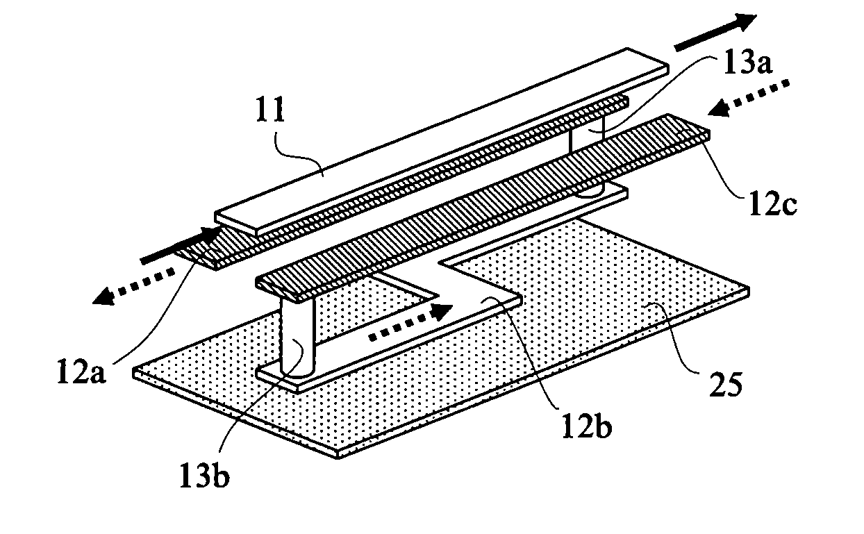
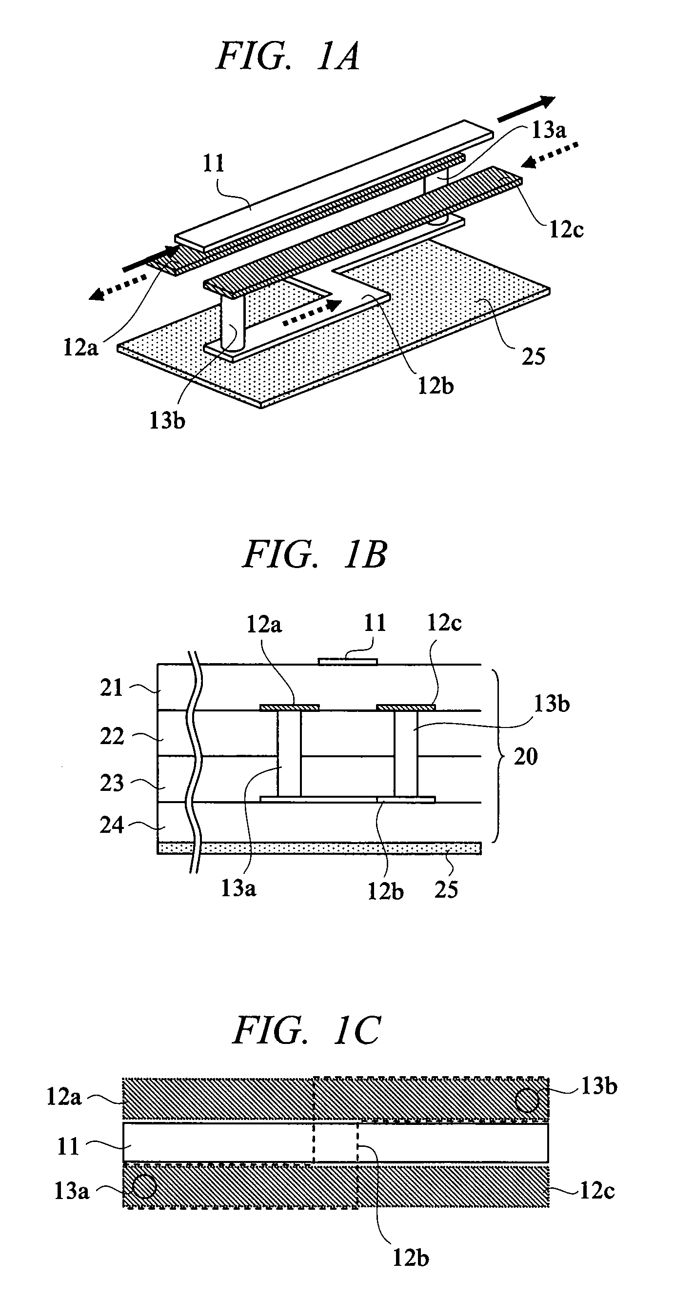
[0051]FIGS. 1A to 1C show a structure of a directional coupler according to a first embodiment of the present invention. FIG. 1A is a perspective diagram of the directional coupler, FIG. 1B is a cross-sectional diagram thereof, and FIG. 1C is a top transparent diagram viewed from top thereof. As can be seen from FIG. 1B, the directional coupler is formed of a multi-layer substrate 20 composed of four insulating layers 21 to 24. In the first embodiment, a glass ceramic multi-layer substrate having a relative permittivity of 7.8 and tanδ of 0.002 is used for the multi-layer substrate. Each insulating film has a thickness of 150 μm. The multi-layer substrate 20 is provided with a ground plane 25 on the back surface. Conductivity of a wiring conductor including the ground plane is 4×10⁷S / m, and a thickness thereof is 15 μm. A main-line 11 is provided on a front surface, which is an opposite side of the back surface where the ground plane of the multi-layer substrate is provided. A sub-l...

second embodiment

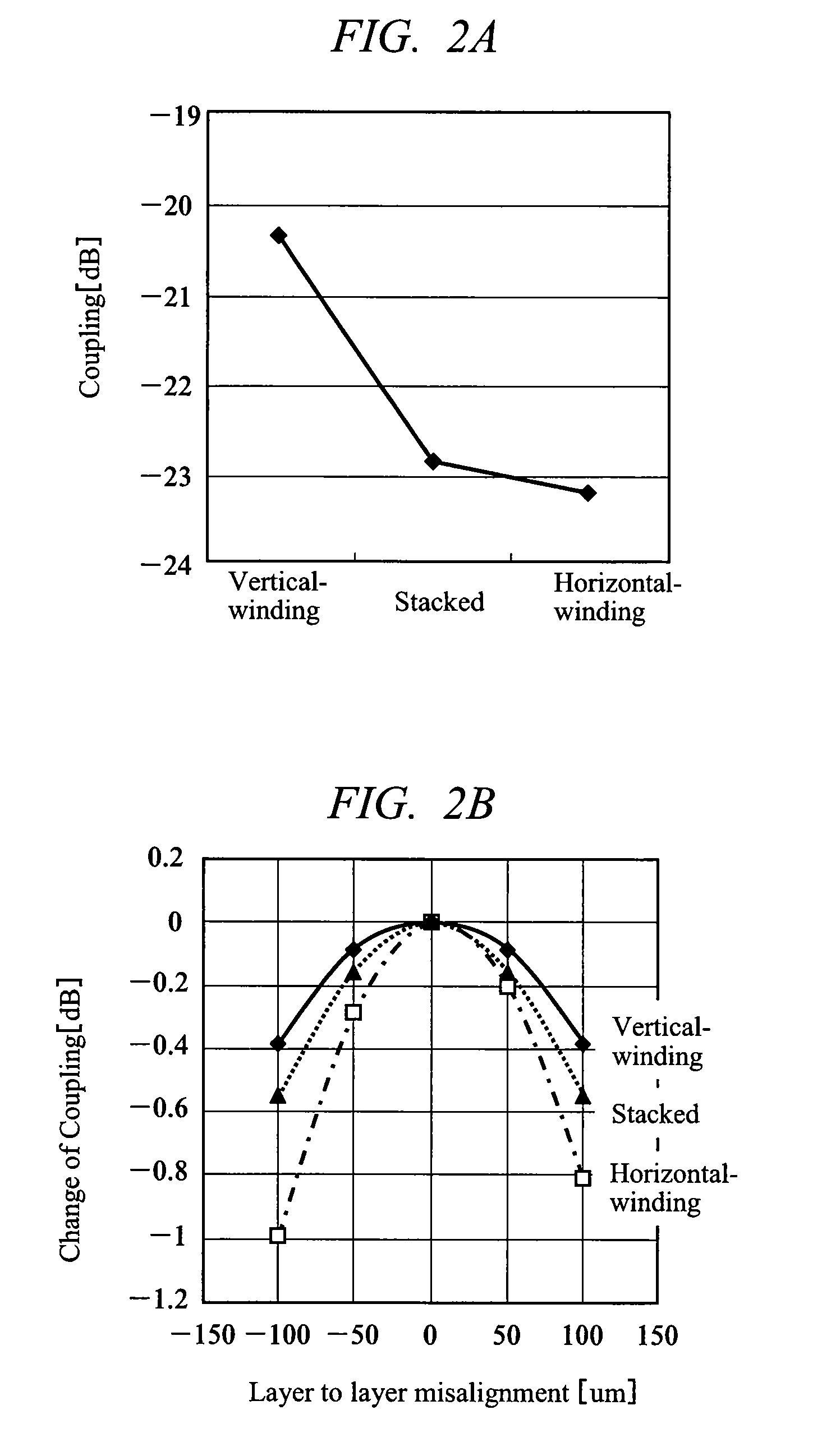
[0061]A directional coupler according to a second embodiment has a structure in which the directional coupler according to the first embodiment is used and directivity is adjusted further. The structure of the directional coupler according to the second embodiment is similar to that of the directional coupler according to the first embodiment in the number of the substrate layers, the insulating layer, the thickness and material of the conductor, the line width of the sub-line, and the line length of the main-line contributing to the coupling. A width of the main-line and a distance between portions running parallel of lines forming the sub-line are parameters for improving the directivity.

[0062]FIG. 3A is a graph showing dependence of the coupling and the directivity on the width of the main-line. FIG. 3B is a graph showing dependence of the coupling and the directivity on the distance between the sub-lines. Both of these graphs represent results obtained through a three-dimensiona...

third embodiment

[0065]A directional coupler according to a third embodiment is achieved by further applying the structure of the vertical winding type described in the first embodiment. FIGS. 4A to 4C show an example of a structure of a directional coupler according to the third embodiment of the present invention. FIG. 4A is a perspective diagram of the directional coupler, FIG. 4B is a cross-sectional diagram thereof, and FIG. 4C is a top transparent diagram viewed from top thereof. The number of substrate layers, insulating layer, thickness and material of the conductor, width of the main-line and the sub-line, a line length of the main-line contributing to coupling, and the like forming the directional coupler according to the third embodiment are identical to those according to the first embodiment. Difference between the third embodiment and the first embodiment is that, in the third embodiment, as shown in FIGS. 4A to 4C, a line 12a of the sub-line is provided on a layer immediately under th...


PUM


Abstract

A directional coupler with a high coupling per unit area and small variations in characteristic at manufacturing capable of achieving a high directivity easily and an RF circuit module provided with the directional coupler are achieved. A main-line is provided on a front surface of a multi-layer substrate, a ground plane is provided on a back surface of the multi-layer substrate. On an inner layer immediately under the main-line, two lines in parallel with the main-line are provided, and one line is provided on a layer closer to the ground plane than the two lines. By connecting the two lines and the one line with vias, a sub-line with a shape of a winding of a loop is formed. In the sub-line, a main component of a vector vertically penetrating the loop is horizontal with respect to the ground plane.

Description

CROSS-REFERENCE TO RELATED APPLICATION[0001]The present application claims priority from Japanese Patent Application No. JP 2006-253850 filed on Sep. 20, 2006, the content of which is hereby incorporated by reference into this application.FIELD OF THE INVENTION[0002]The present invention relates to a directional coupler and an RF circuit module, and particularly, to a directional coupler suitable for application detecting transmission signal power in a wireless communicator and an RF circuit module including the directional coupler.BACKGROUND OF THE INVENTION[0003]An example of a directional coupler which detects an output of an RF circuit module reliably and accurately is disclosed in Japanese Patent Application Laid-Open Publication No. 2002-43813 (Patent Document 1). In this example, the directional coupler that detects the output of the RF circuit module has a structure in which a main-line and a sub-line overlap each other via a dielectric. And, the width of the main-line is na...

Claims


Application Information

Patent Timeline
Patent Type & Authority Applications(United States)
IPC IPC(8): H04B1/04H01P3/08H01P5/18
CPCH01P5/184H01P5/18
Inventor OKABE, HIROSHI
Owner RENESAS ELECTRONICS CORP
Why Eureka
Try Eureka