Semiconductor package and method of fabricating the same

Active Publication Date: 2013-03-28
SILICONWARE PRECISION IND CO LTD
View PDF6 Cites 14 Cited by
  • Summary
  • Abstract
  • Description
  • Claims
  • Application Information

AI Technical Summary

Benefits of technology

[0008]It can be seen from the above that the semiconductor package of the present invention is obtained by stacking, that is, forming the electronic element on the cap, forming the first conductive pads and the second conductive pads on the electronic element, and forming the first conductive elements on the first conductive pads and electrica

Problems solved by technology

However, in contrast to the traditional semiconductor chips, surface components of the MEMS chip are easy to damage by environmential influence to cause reliability problem, so the cost of the MEMS package

Method used


Image

  • Semiconductor package and method of fabricating the same
  • Semiconductor package and method of fabricating the same
  • Semiconductor package and method of fabricating the same

Examples


first embodiment

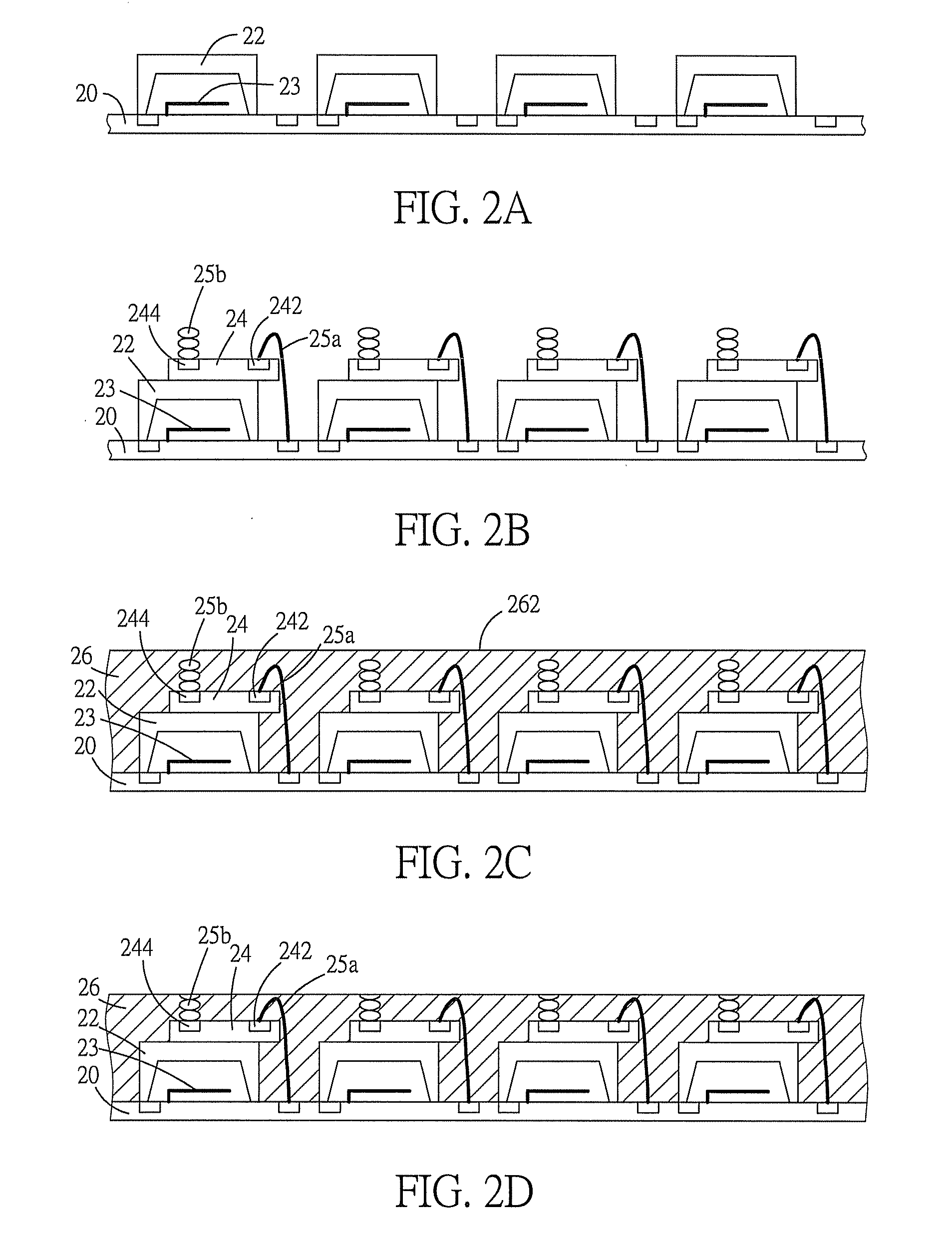
[0015]A semiconductor package and a method of fabricating the same disclosed by the present invention are described in details in conjunction with FIGS. 2A to 2E

[0016]As shown in FIG. 2A, a substrate 20 with a plurality of micro electro mechanical system (MEMS) element 23 is provided. A cap 22 is provided on the substrate 20 for covering the MEMS element 23. The cap 22 can be made of, but not limited to, glass, silicon, metal, ceramic or epoxy resin. The cap 22 can be bonded to the substrate 20 via an adhesive, such as glass frit or resin, or by anodic bonding, eutectic bonding, or silicon fusion bonding techniques. After the cap is bonded, the cavity of the cap can be vacuumed to stay in a hermeticity or non-hermeticity state.

[0017]As shown in FIG. 2B, an electronic element, such as, but not limited to a semiconductor chip 24, is provided on the cap 22 in a staggered manner with respect to the cap 22. In another embodiment, an active element, a passive element or other electronic e...

second embodiment

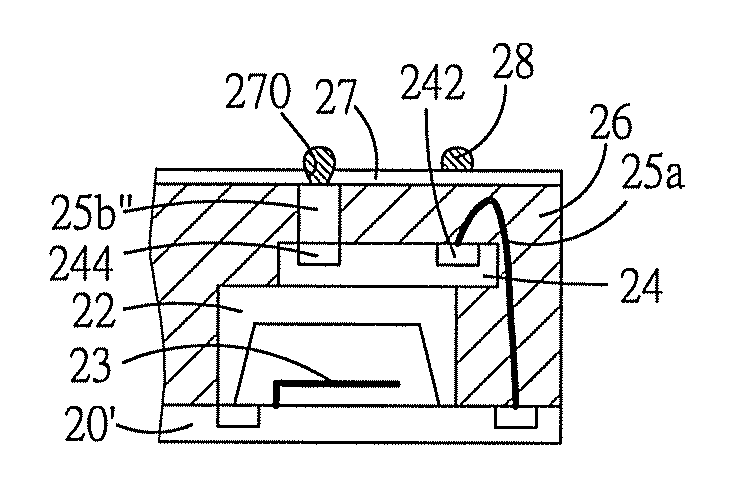
[0023]Referring to FIG. 3A to 3C, a method of fabricating a semiconductor package according to a second embodiment of the present invention is provided. This embodiment shows that the second conductive elements are bonding wires.

[0024]As shown in FIG. 3A, which is a continuation of FIG. 2B, second conductive elements 25b′ such as bonding wires are formed on the second conductive pads 244. One end of each of the bonding wires is attached to the cap 22. The bonding wires are connected to the second conductive pads 244 by the wire bonder, and then vertically stretched to a height less than about 100 μm, and connected to the cap 22. The vertically stretched height of the bonding wires are determined by various implementations, but the overall height is less than 100 μm.

[0025]As shown in FIG. 3B, the encapsulant 26 is formed on the substrate 20, with the second conductive elements 25b′ being exposed therefrom. The bonding wires and a portion of the bonding wires exposed from the encapsul...


PUM


Abstract

A semiconductor package is provided, which includes: a micro electro mechanical system (MEMS) chip; a cap provided on the MEMS chip; an electronic element provided on the cap including a plurality of first conductive pads and second conductive pads; a plurality of first conductive elements electrically connected to the first conductive pads and the MEMS chip; a plurality of second conductive elements formed on the second conductive pads, respectively; and an encapsulant formed on the MEMS chip covering the cap, the electronic element, the first conductive elements and the second conductive elements, with the second conductive elements being exposed from the encapsulant. Thus, the size of the semiconductor package is reduced. A method of fabricating the semiconductor package is also disclosed.

Description

FIELD OF THE INVENTION[0001]The present invention relates to semiconductor packages and methods of fabricating the same, and, more particularly, to a semiconductor package having MEMS elements and a method of fabricating the same.BACKGROUND OF THE INVENTION[0002]With the rapid development of semiconductor processes, low-profiled and compact-sized electronic components come to the market. Recently, it is popular in the art to integrate various mechanical components with electronic components to produce a nanometer scale product. Therefore, a micro electro mechanical system (MEMS) is developed, which involves manufacturing traditional mechanical components using a patterning method (such as exposure, development, etching, etc.) of the semiconductor manufacturing process to obtain miniaturized components. With these components converting environmental signals to electrical signals, signals are obtained by electrical conversion. These components are, for example, pressure sensors, flow ...

Claims


Application Information

Patent Timeline
IPC IPC(8): H01L23/04H01L21/50
CPCB81C1/0023B81B2207/012B81B2207/098H01L2224/48091H01L2924/1461H01L2924/00014H01L2924/00
Inventor CHANG, HONG-DALIAO, HSIN-YI
Owner SILICONWARE PRECISION IND CO LTD
Why Eureka
Try Eureka