Functional Film Containing Structure And Method Of Manufacturing Functional Film

Inactive Publication Date: 2008-03-27
FUJIFILM CORP
View PDF9 Cites 12 Cited by
  • Summary
  • Abstract
  • Description
  • Claims
  • Application Information

AI Technical Summary

Benefits of technology

[0012] In view of the above-mentioned problems, a first purpose of the present invention is to provide a method of manufacturing a functional film by which a functional film formed on a film formation substrate can be

Problems solved by technology
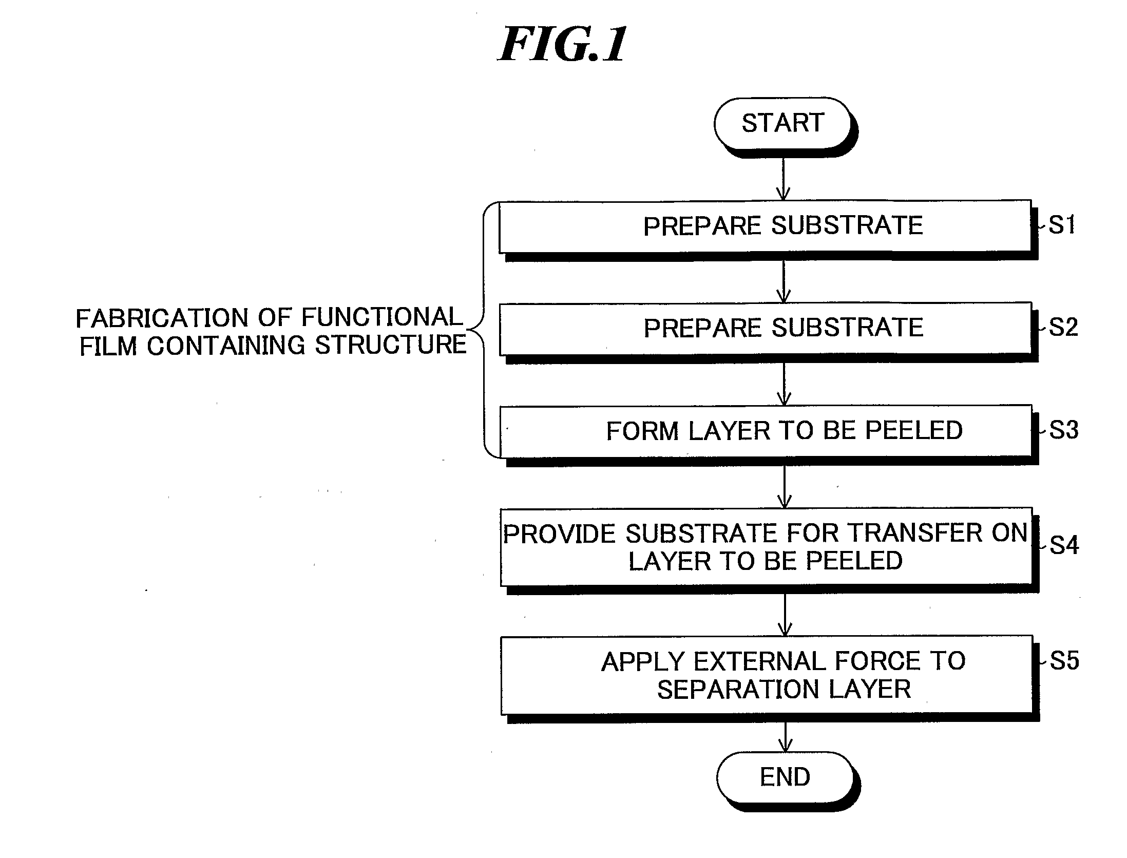
However, there has been a problem that a film of function material (also simply referred to as “functional film”) formed by film formation does not sufficiently exert its function in a condition after the film formation, and the film is inferior to a bulk material in performance.
However, according to JP-A-54-94905, since the release layer is removed by oxidation reaction,

Method used


Image

  • Functional Film Containing Structure And Method Of Manufacturing Functional Film
  • Functional Film Containing Structure And Method Of Manufacturing Functional Film
  • Functional Film Containing Structure And Method Of Manufacturing Functional Film

Examples


example

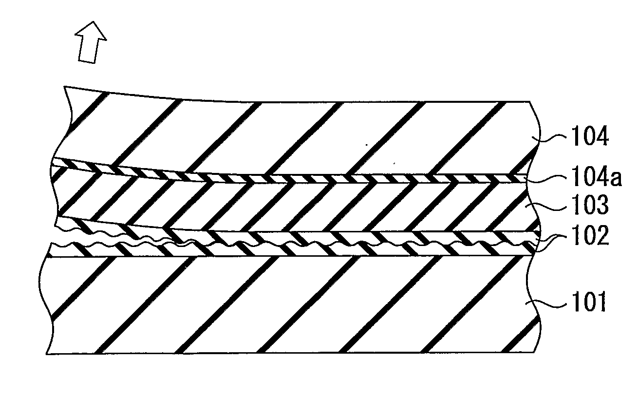
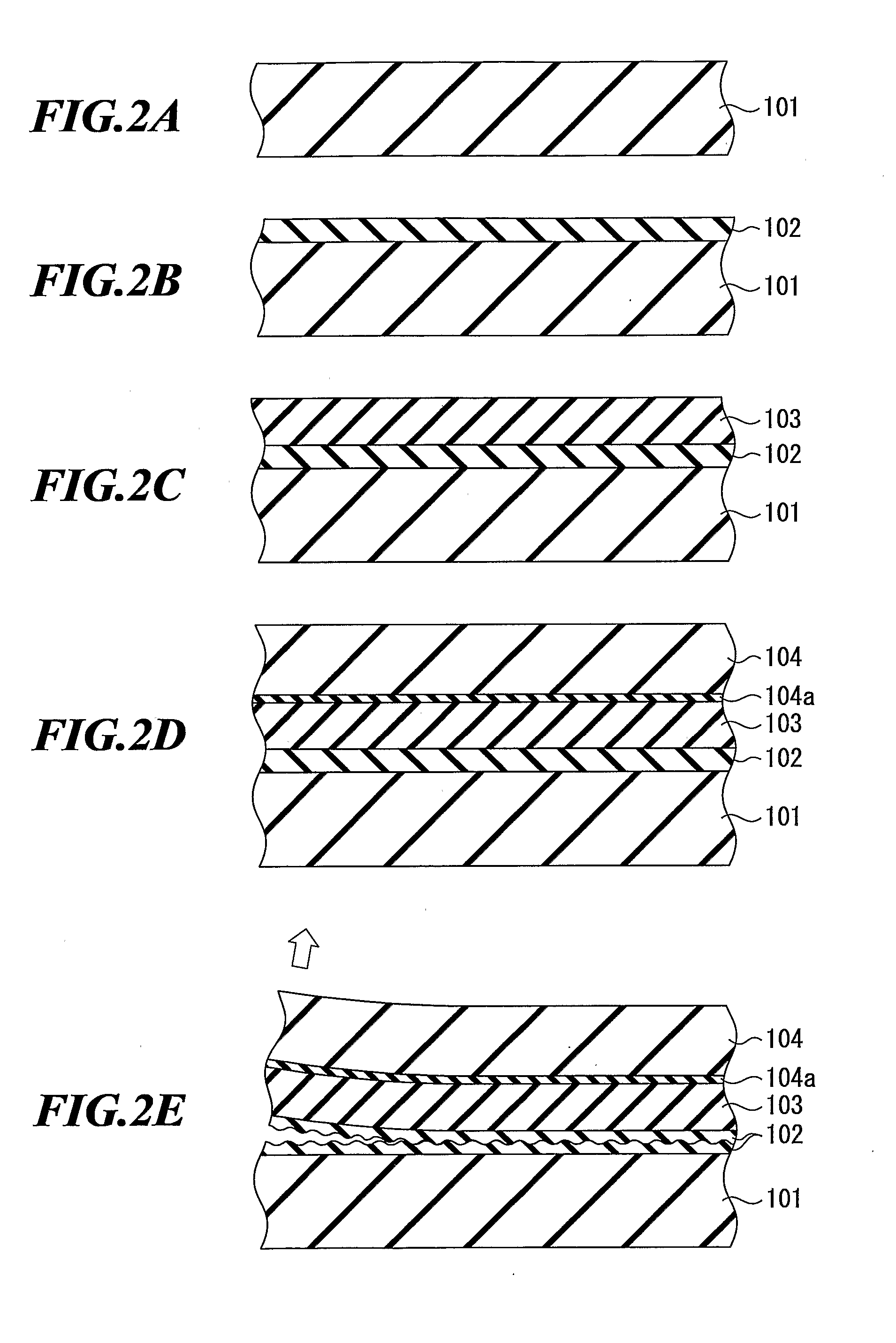
[0106] An h-BN film having a thickness of about 0.5 μm is formed as a separation layer by using boron trichloride (BCl3) and ammonia (NH3) as raw materials according to thermal CVD (substrate temperature 1200° C.). A lower electrode of platinum (Pt) is formed on the h-BN film by the sputtering method, and a PZT (lead zirconate titanate) film having a thickness of about 2 μm is formed thereon by the sputtering method. At this time, the substrate is heated to a temperature of about 550° C. Furthermore, an upper electrode of platinum is formed on the PZT film by using the sputtering method, and thereby, a Pt / PZT / Pt piezoelectric element is fabricated.

[0107] Then, an adhesive agent is applied onto the upper electrode of the Pt / PZT / Pt piezoelectric element formed on the quartz substrate, and an epoxy substrate is bonded as a substrate for transfer. Further, when the quartz substrate is fixed and an external force is applied to the separation layer by pulling up the epoxy substrate, frac...


PUM

PropertyMeasurementUnit
Forceaaaaaaaaaa
Structureaaaaaaaaaa
Adhesivityaaaaaaaaaa

Abstract

A method of manufacturing a functional film by which a functional film formed on a film formation substrate can be easily peeled from the film formation substrate. The method includes the steps of: (a) forming a separation layer (102) on a substrate (101); (b) forming a layer to be peeled (103, 105, 106) containing a functional film (103, 105b, 106a), which is formed by using a functional material, on the separation layer (102); and (c) applying an external force to the separation layer (102) to produce fracture within the separation layer (102) or at an interface thereof so as to peel the layer to be peeled (103, 105, 106) from the substrate (101) or reduce bonding strength between the layer to be peeled (103, 105, 106) and the substrate (101).

Description

TECHNICAL FIELD [0001] The present invention relates to a method of manufacturing a functional film including a dielectric material, piezoelectric material, pyroelectric material, magnetic material, semiconductor material or the like, and a functional film containing structure to be used in a manufacturing process of the functional film. BACKGROUND ART [0002] Recent years, in response to the needs for electronic devices such as miniaturization, speeding up, integration, and multifunctionality, the manufacture of devices containing functional materials such as electronic ceramics, which express predetermined functions by being applied with electric fields or magnetic fields and include a dielectric material, piezoelectric material, magnetic material, pyroelectric material and semiconductor material, by using various film formation technologies has been actively studied. [0003] For example, in order to enable high-definition and high-quality printing in an inkjet printer, it is necess...

Claims


Application Information

Patent Timeline
IPC IPC(8): B32B3/00B05D3/00B05D3/10B05D5/12B32B9/04B32B15/04B32B17/06H01L21/02H01L21/20H01L21/8246H01L27/105H01L41/18H01L41/187H01L41/22H01L41/312H01L41/332H01L41/39
CPCY10T428/24612H01L21/76251Y10T428/31678Y10T428/31504H10N60/0296H10N30/074H10N30/073
Inventor SAKASHITA, YUKIO
Owner FUJIFILM CORP
Why Eureka
Try Eureka