Material of over voltage protection device, over voltage protection device and manufacturing method thereof

a protection device and material technology, applied in the direction of current responsive resistors, varistors, varistors, etc., can solve the problems of difficult design of devices on chips, large volume of closed containers, and abnormal energy conducted to ground lines, etc., to reduce over voltage, reduce over voltage, and reduce the effect of trigger voltag

Inactive Publication Date: 2008-04-03
INPAQ TECH
View PDF16 Cites 44 Cited by
  • Summary
  • Abstract
  • Description
  • Claims
  • Application Information

AI Technical Summary

Benefits of technology

[0023]The material and structure of the present invention is basically equivalent to a mechanism of the point discharge principle and a gas discharge device, thus having the advantages of a low trigger voltage and a long service life. Furthermore, the material and structure of the present invention can be fabricated as a chip device by using a conventional commercialized process.
[0024]The over voltage protection device manufactured according to the present invention can easily achieve an electrode gap less than 5 μm without using precise processing equipment and can provide a large number of discharge positions, thereby greatly reducing over voltages generated when abnormal charges enter a system.
[0025]According to the material of the over voltage protection device of the present invention and the fired structure thereof, as the base matrix is a non-conductive material, and does not have the P-N interface or a mixed structure of P powders and N powders, the discharge energy is released only through the discharge positions, and the matrix of the present invention has no interface to be destroyed. Therefore, the device manufactured according to the present invention has a long service life.

Problems solved by technology

When abnormal charges enter the device (i.e., an over voltage is generated), a transient change from high resistance to low resistance occurs, and thus an intruding abnormal energy is conducted to a ground line.
Furthermore, since the discharge will generate heat, the closed container usually has a large volume for heat dissipation.
Therefore, it is difficult to design the device on a chip, and the current requirements for light, thin, short, and small designs cannot be met.
However, unlike other over voltage protection devices, the protection device adopting the point discharge principle has a hollow state between the two electrodes when discharging.
Since the energy must enter the semiconductors or semiconductor oxides, after multiple actuations, the phenomena of breakdown, reduced resistance, increased leakage current, and short circuits often occur, thereby reducing the service life.
Therefore, this method has constraints on equipment cost and electrode clearance.
However, not all the materials with the P-N interface can bear the discharge energy, the service life may be short and an additional cost must be incurred to develop this base matrix material.
However, in the practical manufacture of the device, since the melting point of zinc oxide is 1700° C., after a long time and multiple discharge impacts, the zinc oxide material sometimes is broken down and then melts.
Therefore, the binder may be burned, and further the two insulating conductors may lose their functions, resulting in a short circuit of the device.
This material structure has some disadvantages in practical application.
Firstly, the thickness of the insulating layer is less than several hundred angstroms, so it is quite difficult to control the thickness in the process.
When the insulating layer is too thin, a short circuit of the device occurs.
The above are the disadvantages when the insulating layer is applied on the surface of a conductor or a semiconductor powder.

Method used


Image

  • Material of over voltage protection device, over voltage protection device and manufacturing method thereof
  • Material of over voltage protection device, over voltage protection device and manufacturing method thereof
  • Material of over voltage protection device, over voltage protection device and manufacturing method thereof

Examples


first embodiment

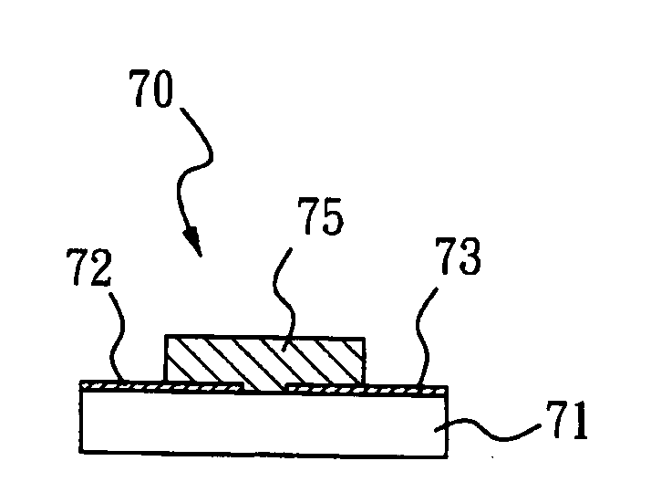
[0058]FIGS. 10 and 11 are a plan view and a side view of an over voltage protection device 100 according to another embodiment of the present invention. In this embodiment, ingredients of a paste 104 are the same as that of the paste 75 in the Firstly, a first electrode 102 is formed on an Al2O3 substrate 101. Then, the paste 104 of the present invention is printed on the first electrode 102, wherein a part of the paste 104 is printed on the first electrode 102, and the rest is printed on the Al2O3 substrate 101. Finally, a second electrode 103 is formed, wherein a part of the second electrode 103 is attached to the paste 104 and the rest is attached to the Al2O3 substrate 101. After the firing treatment at 850° C., the material 104 of the present invention is attached to the Al2O3 substrate 101 and the first electrode 102, and the second electrode 103 is attached to the material 104 and the Al2O3 substrate 101. The first electrode 102 is connected to a system (not shown), and the ...

second embodiment

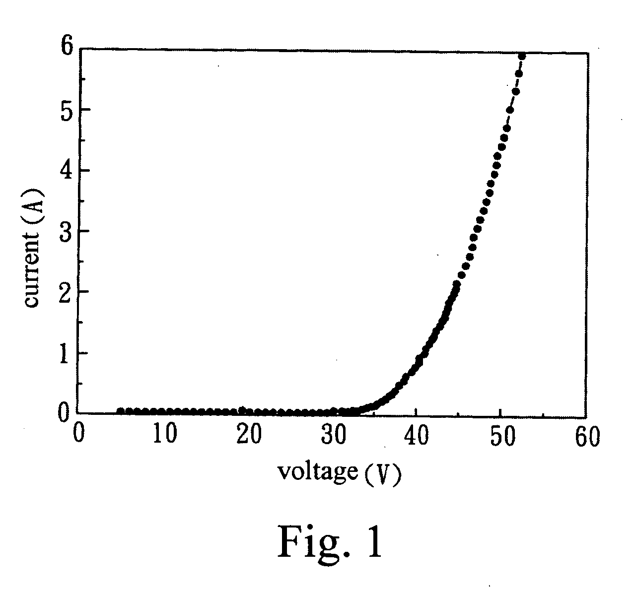
[0059]In another embodiment of the present invention, 15 wt % of Pt powders, 45 wt % of Al2O3 powders, and 15 wt % of glass powders are mixed with 25 wt % of ethyl cellulose resin solution by using a 3-roll mill, so as to form a paste for printing, and then, a structure that is the same as that in the second embodiment is fabricated. The I-V curve in this embodiment is shown in FIG. 13.


PUM


Abstract

The present invention relates to a material of an over voltage protection device and an over voltage protection device manufactured by the material. The material comprises a non-conductive powder, a metal conductive powder, and an adhesive. The over voltage protection device comprises a first electrode, a second electrode, and a porous structure connected between the first electrode and the second electrode. The present invention also relates to a method for manufacturing the over voltage protection device. The present invention also relates to a method of adjusting the breakdown voltage of an over voltage protection device.

Description

BACKGROUND OF THE INVENTION[0001]1. Field of the Invention[0002]The present invention relates to a material and a structure of an over voltage protection device, and also relates to a method for manufacturing the over voltage protection device.[0003]2. Description of the Prior Art[0004]A common over voltage protection device usually is connected in parallel with a system to be protected, and is grounded in a high-resistance state. When abnormal charges enter the device (i.e., an over voltage is generated), a transient change from high resistance to low resistance occurs, and thus an intruding abnormal energy is conducted to a ground line.[0005]The transient change from high resistance to low resistance is also called a device actuation. The voltage observed then is called a breakdown voltage, which is also referred to as a trigger voltage.[0006]Based on the point discharge principle, charges jumping from one conductor to another and usually the trigger voltage are decreased when the...

Claims


Application Information

Patent Timeline
Patent Type & Authority Applications(United States)
IPC IPC(8): H01C7/10
CPCH01C7/105
Inventor LIU, TE-PANGCHANG, HSIU-YUN
Owner INPAQ TECH
Why Eureka
Try Eureka