Electronic Device and Method for Manufacturing the Same

Active Publication Date: 2008-04-03
MURATA MFG CO LTD
View PDF8 Cites 42 Cited by
  • Summary
  • Abstract
  • Description
  • Claims
  • Application Information

AI Technical Summary

Benefits of technology

[0022] The electronic device of the present invention (Claim 1) is an electronic device having an electronic device main body and an external electrode provided on a surface of the electronic device main body, and the external electrode includes: a Cu-baked electrode layer primarily composed of Cu; a Cu plating layer which is formed on the Cu-baked electrode layer and which is processed by a recrystallization treatment; and at least one upper-side plating layer formed on the Cu plating layer which is processed by the recrystallization treatment. Since the texture of the Cu plating layer processed by the recrystallization treatment is dense, a highly reliable electronic device can be obtained that is able to prevent the entry of a plating solution inside a ceramic element via the external electrode and entry of moisture of external environment inside thereof.
[0023] In addition, instead of preventing the entry of a plating solution and moisture of external environment by a dense Cu-baked electrode layer obtained by baking, since the Cu plating layer processed by the recrystallization treatment is provided, the entry of a plating solution and moisture in external environment is prevented by the dense Cu plating layer obtained by the recrystallization. Accordingly, the generation of so-called “glass scum” can be suppressed in which a glass component moves to and precipitates on the surface of the Cu-baked electrode layer when baking is excessively carried out to obtain a dense Cu-baked electrode layer. Hence, as a result, the generation of defects, such as plating defects in a subsequent plating step (such as a Ni plating step or a solder plating step) for forming the upper-side plating layer and/or solder popping defects caused by degradation in denseness of a plating layer to be formed, can be suppressed or prevented.
[0024] In addition, as is the electronic device of Claim 2, in the structure according to Claim 1 of the present invention, when the electronic device main body has a ceramic

Problems solved by technology

Although the Ni plating layers 57a and 57b are to be used as an interlayer function to prevent entry of a Sn plating solution and moisture of external environment, since minute voids are inherently present in the Ni plating layers 57a and 57b, the function of preventing the entry of a plating solution and moisture is not satisfactory.
However, in a baking step in which the Cu-baked electrode layer is densified by baking, glass moves up to the surface of the Cu-baked electrode layer and precipitates thereon, thereby, for example, causing a plating defect in a subsequent step of forming the Ni plating layers 57a and 57b and/or causing solder popping in a mounting step (soldering step) due to degra

Method used


Image

  • Electronic Device and Method for Manufacturing the Same
  • Electronic Device and Method for Manufacturing the Same
  • Electronic Device and Method for Manufacturing the Same

Examples


Example

EXAMPLE 1

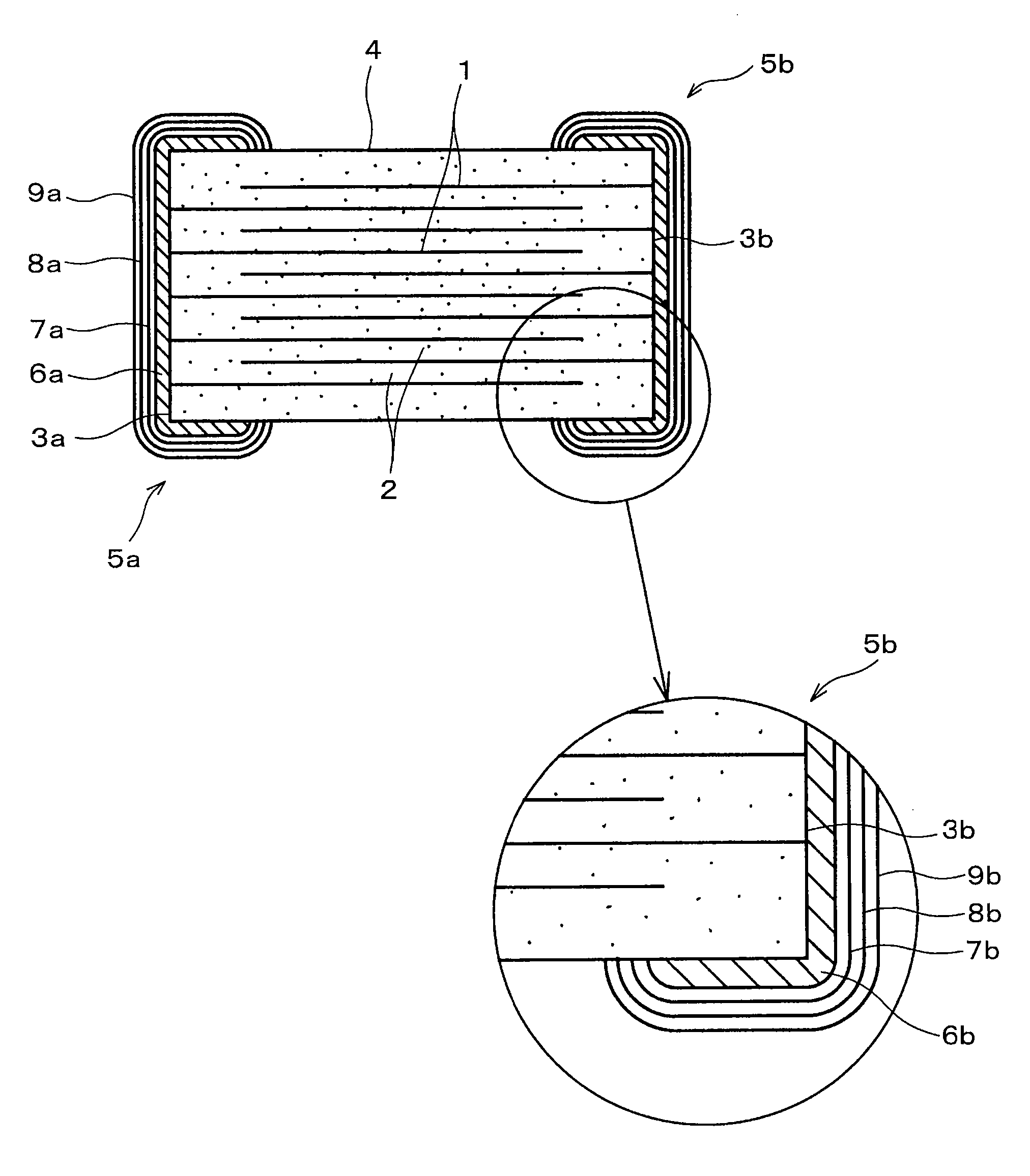
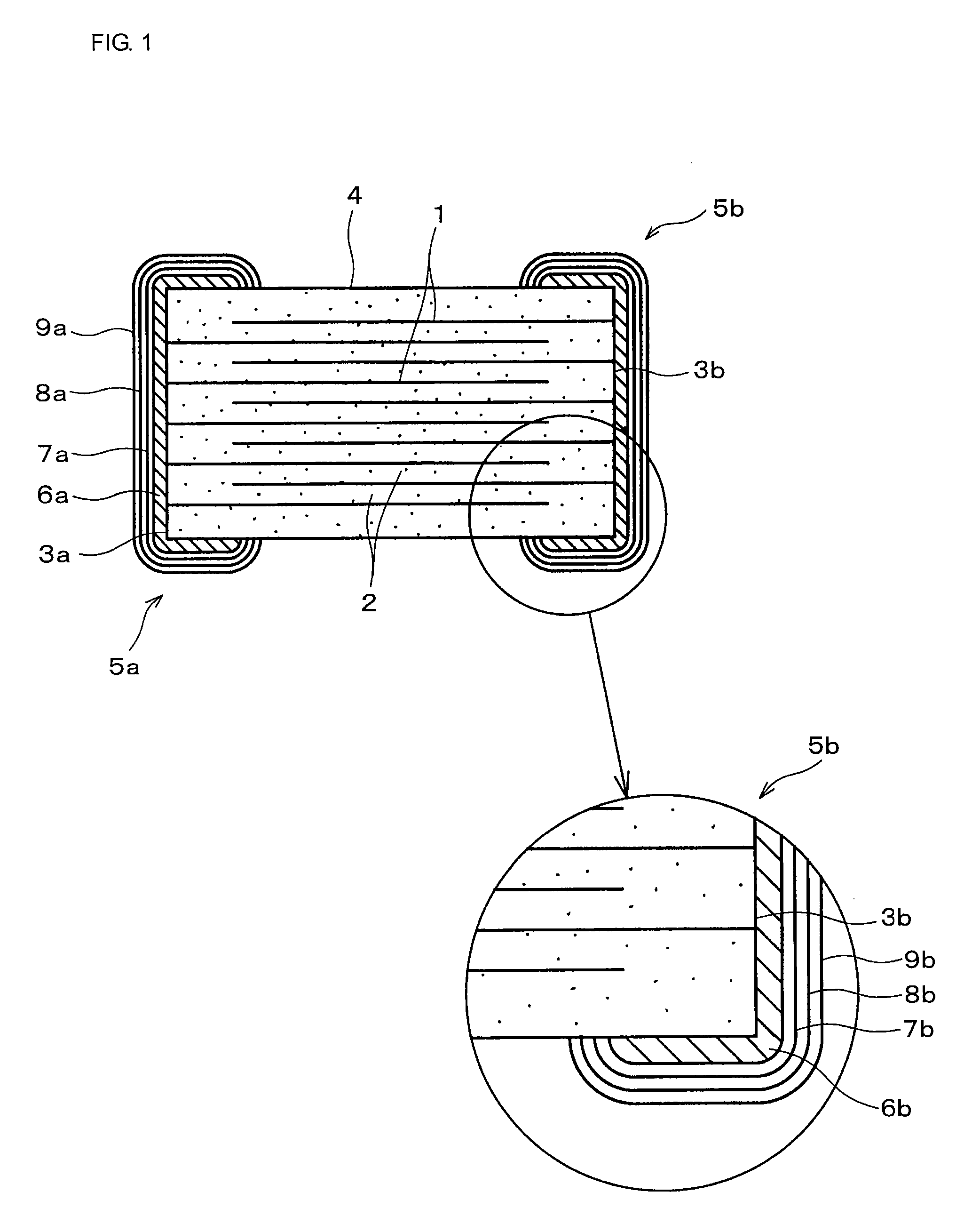
[0040]FIG. 1 is a cross-sectional view showing the structure of an electronic device (multilayer ceramic capacitor in this example) manufactured by a method for manufacturing an electronic device according to an example (example 1) of the present invention.

[0041] This multilayer ceramic capacitor is composed of two external electrodes 5a and 5b and a ceramic element (electronic device main body) 4 having internal electrodes (such as Ni electrodes) 1 which are disposed to face each other with ceramic layers 2 interposed therebetween and which are alternately extended to opposite end surfaces 3a and 3b, and the two external electrodes 5a and 5b are provided for the ceramic element 4 so as to be electrically connected to the internal electrodes 1.

[0042] In addition, in the multilayer ceramic capacitor of this example, the external electrodes 5a and 5b have a four-layered structure including Cu-baked electrode layers 6a and 6b, Cu plating layers 7a and 7b formed thereon, Ni ...

Example

[0064] As shown in Table 1, in the case of the multilayer ceramic capacitors of comparative example 1 which were not processed by the heat treatment (recrystallization treatment), defects were observed in all of 72 samples in the reliability test (PCBT test) The reason for this is believed that the particles of the Cu plating layer were not recrystallized, and hence densification thereof was not advanced.

[0065] In addition, as shown in Table 1, also in the case of the multilayer ceramic capacitors of comparative example 2 which were processed by a heat treatment at 200° C., defects were also observed in all of 72 samples in the reliability test (PCBT test) as in the case of comparative example 1 in which the heat treatment (recrystallization treatment) was not performed. The reason for this is believed that since the temperature was low by a heat treatment at 200° C. for 20 minutes, although the average particle diameter of the Cu particles forming the Cu plating layer was increase...

Example

[0068] In particular, in the case of the multilayer ceramic capacitors of example 3 in which the heat treatment (recrystallization treatment) was performed at 600° C. for 20 minutes (example 3), in all of the plating test, the reliability test, and the solder popping test, no defects were observed, and hence the most preferable result was obtained. The reasons for this are believed that in the heat treatment performed at 400° C. (example 1) and at 500° C. (example 2), a Cu plating layer having a dense texture capable of completely preventing the entry of a plating solution and moisture could not be obtained, and that on the other hand, when the heat treatment temperature was increased to 600° C., the recrystallization of the Cu plating layer was further advanced, and the texture thereof was changed to a more dense structure.

[0069] In the examples described above, although the multilayer ceramic capacitors are described by way of example, the present invention can be applied to, bes...


PUM

PropertyMeasurementUnit
Temperatureaaaaaaaaaa

Abstract

A highly reliable electronic device and a method for manufacturing the same are provided, the electronic device preventing entry of a plating solution via an external electrode and entry of moisture of external environment inside thereof, and generating no soldering defects nor solder popping defects which are caused by precipitation of a glass component on a surface of the external electrode.
The structure is formed of Cu-baked electrode layers 6a and 6b primarily composed of Cu, Cu plating layers 7a and 7b which are formed on the Cu-baked electrode layers 6a and 6b and which are processed by a recrystallization treatment, and upper-side plating layers 9a and 9b formed on the Cu plating layers 7a and 7b.
After the Cu plating layers 7a and 7b are formed, a heat treatment is performed at a temperature in the range of a temperature at which the Cu plating layers 7a and 7b are recrystallized to a temperature at which glass contained in a conductive paste is not softened (both inclusive), so that the Cu plating layers 7a and 7b are recrystallized.

Description

CROSS REFERENCE TO RELATED APPLICATIONS [0001] The present application is a continuation of International Application No. PCT / JP2006 / 310389, filed May 24, 2006, which claims priority to Japanese Patent Application No. JP2005-164841, filed Jun. 3, 2005, the entire contents of each of these applications being incorporated herein by reference in their entirety.FIELD OF THE INVENTION [0002] The present invention relates to an electronic device and a method for manufacturing the same, and more particularly, relates to an electronic device having the structure in which an external electrode is formed on a surface of an electronic device main body and to a method for manufacturing the electronic device. BACKGROUND OF THE INVENTION [0003] For example, as shown in FIG. 2, a multilayer ceramic capacitor, one of representative ceramic electronic devices, has a ceramic element 54 and two external electrodes 55a and 55b provided on two end portions thereof. The ceramic element 54 has internal el...

Claims


Application Information

Patent Timeline
IPC IPC(8): B32B15/04B05D7/00
CPCH01G4/30H01G4/2325Y10T428/31678H01G4/12
Inventor KATSUBE, HIROSHINISHIKAWA, JUN
Owner MURATA MFG CO LTD
Why Eureka
Try Eureka