

Electrophotographic photoconductor, and electrophotographic apparatus
a photoconductor and electrophotography technology, applied in the field of electrophotography photoconductor and electrophotography apparatus, can solve the problems of high production cost of amorphous silicone photoconductor, electrical discharge hazard, scratched parts and alteration, etc., and achieve good surface smoothing and high abrasion resistance
- Summary
- Abstract
- Description
- Claims
- Application Information
AI Technical Summary
Benefits of technology
Problems solved by technology
Method used
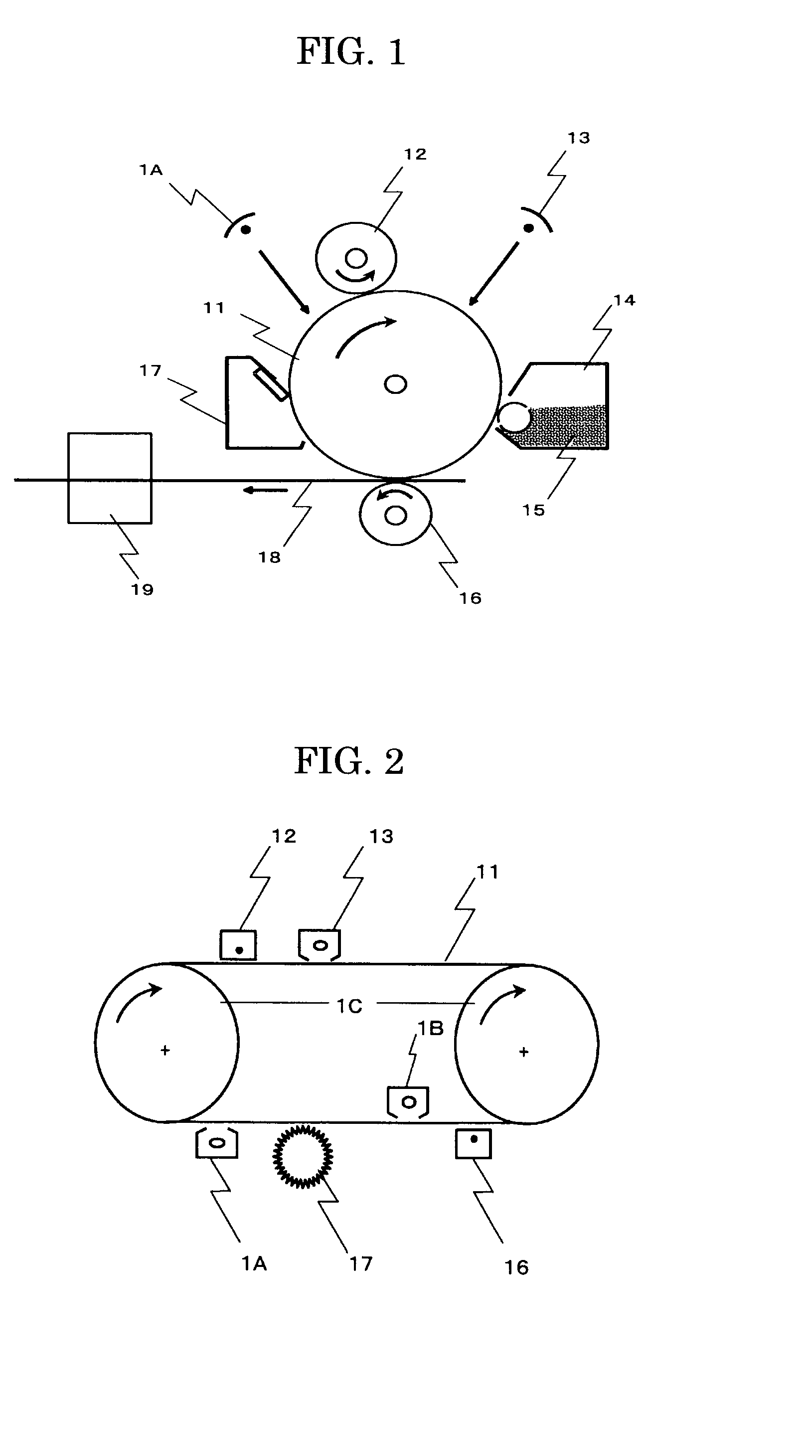
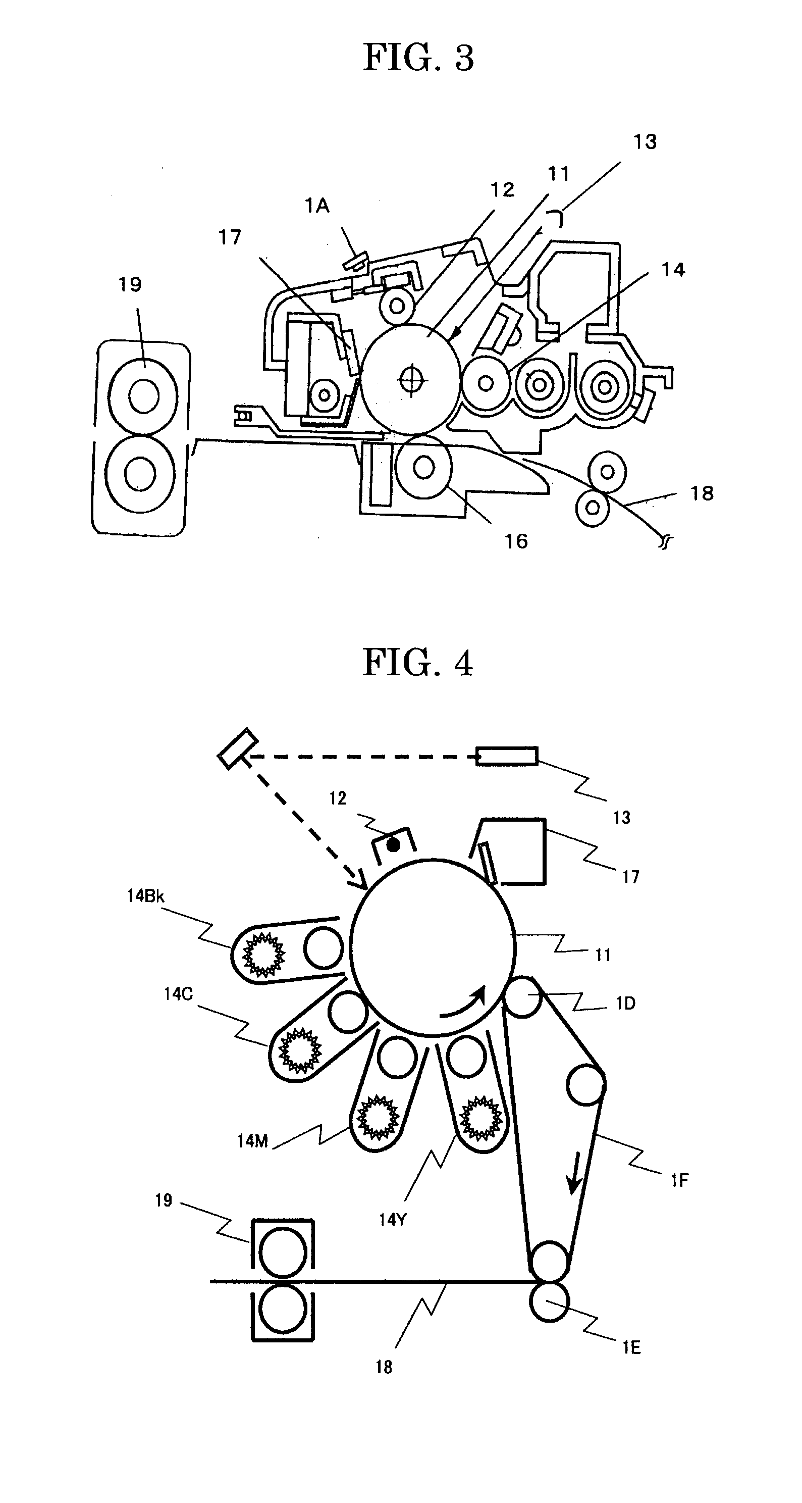
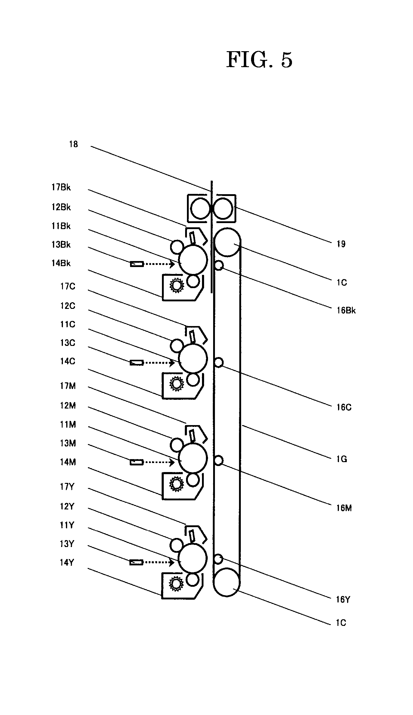
Image

Examples
example 1
[0168] An underlying layer coating liquid, charge generating layer coating liquid, and charge transport layer coating liquid having compositions described below were sequentially applied to an aluminum drum having a radial thickness of 0.8 mm, length of 340 mm, and outer diameter of +30 mm followed by drying, whereby an underlying layer of 3.5 μm thickness, a charge generating layer of 0.2 μm thickness, and a charge transport layer of 22 μm thickness were formed.
[0169] Thereafter, a cross-linked resin surface layer coating liquid having the composition described below was applied by spraying on the charge transport layer. Subsequently, UV curing was applied on the resultant charge transport layer with a space of 120 mm provided between a UV curing lamp and photoconductor while the drum is being rotated. The illumination intensity of the UV curing lamp at this time was 600 mW / cm2 (measured using an accumulated UV meter, UIT-150 produced by Ushio Inc.).
[0170] The rotation speed of t...
example 2
[0189] An electrophotographic photoconductor was obtained in the same manner as Example 1 except that the composition of the cross-linked resin surface layer coating liquid was changed to the following component. The film thickness of the cross-linked resin surface layer was 3 μm.
[Composition of cross-linked resin surface layer coating liquid]Trimethylolpropane triacrylate 30 parts by mass(KAYARAD TMPTA, manufactured by Nippon Kayaku Co.,Ltd.)Cross-linked charge transport material represented by the following 30 parts by massstructural formula (4)Melamine 50 parts by mass(solid content 30 parts by mass)(Super Bekkamine G-821-60, manufactured by Dainippon Inkand Chemicals, Inc.)1-hydroxycyclohexyl phenylketone 1.5 parts by mass(Irgacure 184, manufactured by Ciba specialty chemicals)Silicone compound 7 parts by mass(X-22-174-DX, manufactured by Shin-Etsu Chemical Co., Ltd.)Silicone compound removing material 3 parts by mass(AFC-G, manufactured by Neos Co., Ltd.)Tetrahydrofuran600 pa...
example 3
[0203] An electrophotographic photoconductor was obtained in the same manner as Example 2 except that the component of the cross-linked charge transport material in the composition of the cross-linked resin surface layer coating liquid was changed to the component represented by the following structural formula (5). The test was carried out in entirely the same manner as Example 2.
[0204] As a result, the outline of the dot images was clear, and there is no problem for actual use. As for the thin-line image, pair lines depicted every one dot could be identified.
[0205] Image noise resulting from cleaning defect was not detected on output images.
[0206] The surface roughness Rmax of the photoconductors set in the respective developing stations at the test end time was 0.2 μm at maximum, which means that the surface maintains its smoothness. Further, the abrasion amount of the photoconductor surface at the test end time was 1.3 μm. The static friction coefficient at the test end time...
PUM
| Property | Measurement | Unit |
|---|---|---|
| thickness | aaaaa | aaaaa |
| thickness | aaaaa | aaaaa |
| thickness | aaaaa | aaaaa |
Abstract
Description
Claims
Application Information