

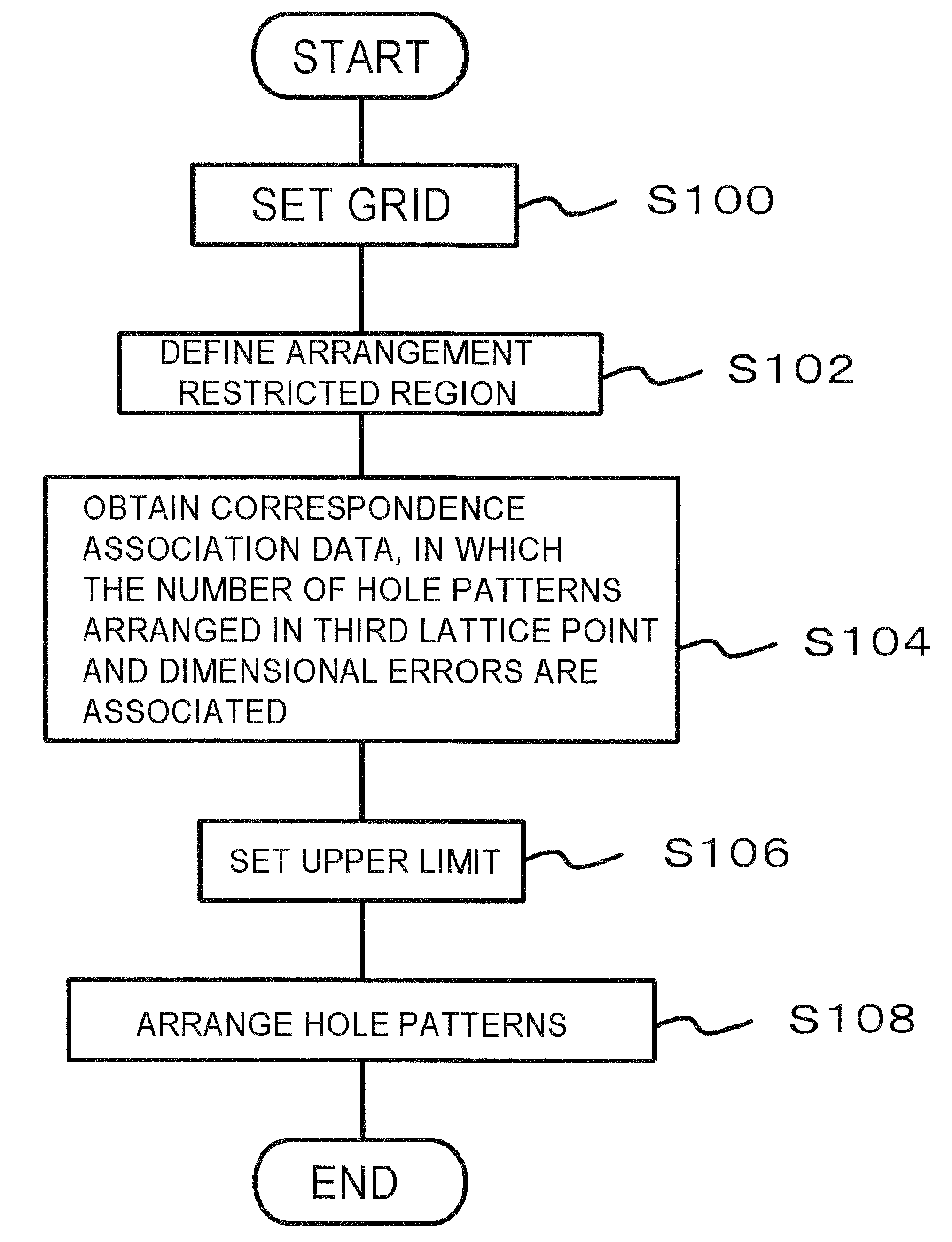
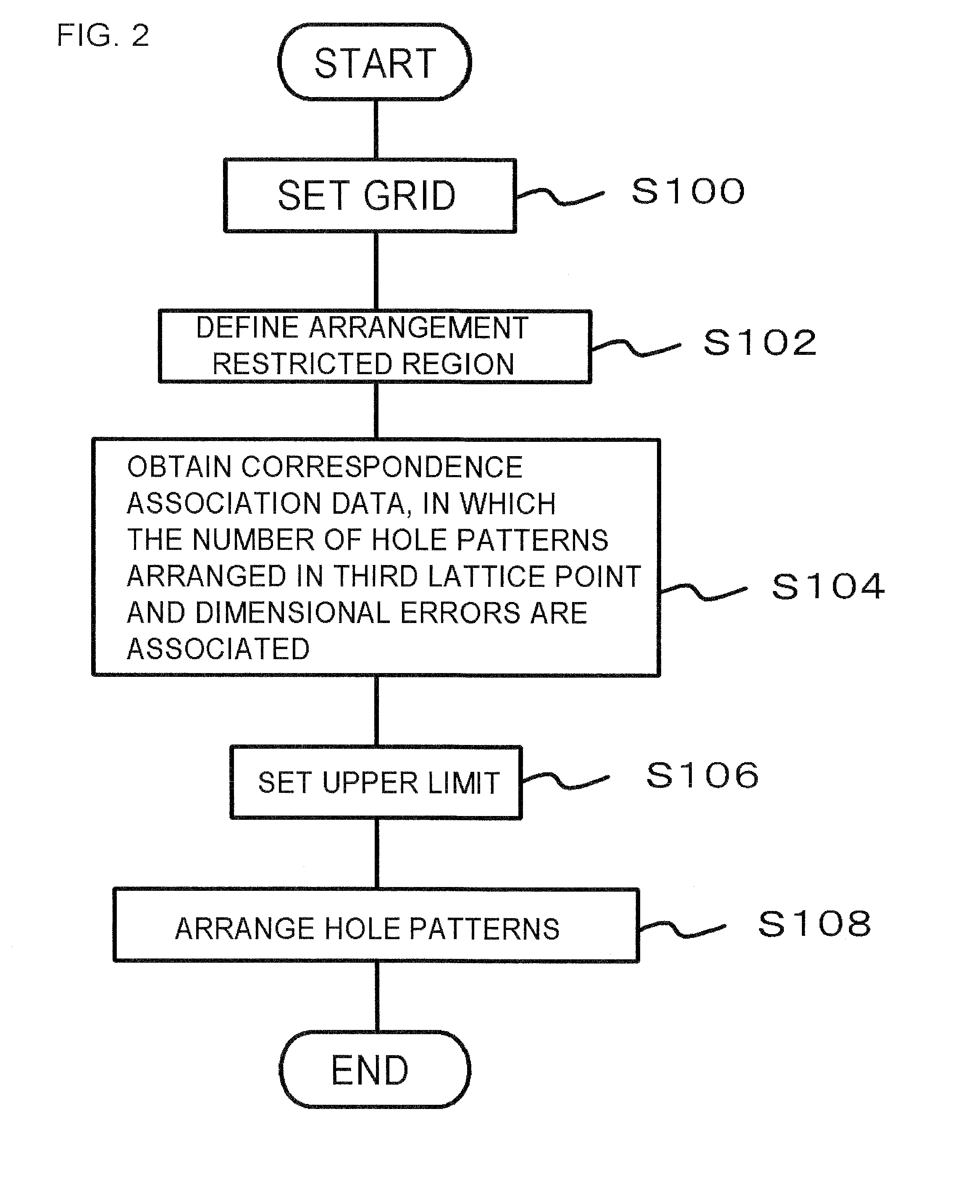
Method of designing a pattern
a pattern and pattern technology, applied in the field of pattern design, can solve the problem of larger dimensional errors, and achieve the effect of reducing the area of the circuit pattern and improving the dimensional accuracy of the hole pattern
- Summary
- Abstract
- Description
- Claims
- Application Information
AI Technical Summary
Benefits of technology
Problems solved by technology
Method used
Image

Examples
first embodiment
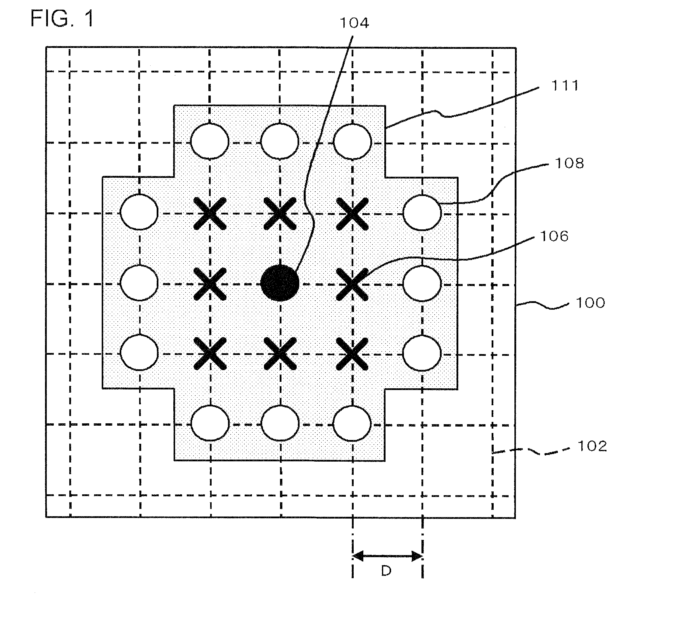
[0028]FIG. 1 is a view showing a pattern drawing of a semiconductor integrated circuit according to the present embodiment.
[0029]In a pattern drawing 100, a grid 102 of an interval smaller than a minimum permissible pitch “d” according to a design rule for the semiconductor integrated circuit is provided. Here, the interval “D” of the grid 102 may be set to D=d / 2.
[0030]Here, it is assumed that a lattice point on which a hole pattern is arranged is a first lattice point 104, a plurality of lattice points which are on the periphery of the first lattice point 104 and are adjacent to the first lattice point 104 are a second lattice point group 106 and a plurality of lattice points which are on the periphery of the second lattice point group 106, and are within a predetermined distance “L” from the first lattice point 104 are a third lattice point group 108. In the present embodiment, it is assumed that a region including the first lattice point 104, the second lattice point group 106, a...
second embodiment
[0045]The present embodiment differs from the first embodiment in a point that a predetermined distance “L” is set to (8)1 / 2×D when defining an arrangement restricted region 111. Other than that, the embodiment is similar to the first embodiment.
[0046]FIG. 5 is a view showing a pattern drawing for a semiconductor integrated circuit according to the embodiment. In this case, a number of lattice points included in a third lattice point group 108 is “16”.
[0047]FIG. 6 is a view showing examples of a pattern drawing 100, in each of which one, two, or three hole patterns 112 are arranged in the third lattice point group 108 for the hole pattern 110 arranged at a first lattice point 104. Here, only a part of conceivable pattern drawings is shown in FIG. 6.
[0048]Also in the present embodiment, when a plurality of patterns are conceivable in order to arrange a certain number of hole patterns, the following processing is performed for all patterns respectively: a reticle is made, patterning o...
PUM
| Property | Measurement | Unit |
|---|---|---|
| diameter | aaaaa | aaaaa |
| diameter | aaaaa | aaaaa |
| diameter | aaaaa | aaaaa |
Abstract
Description
Claims
Application Information