Solid-state imaging device and method of manufacturing the same

a solid-state imaging and imaging device technology, applied in the direction of solid-state devices, final product manufacturing, basic electric elements, etc., can solve the problems of abnormal output values and image quality degradation, and achieve the effects of reducing the occurrence of white spots and dark current, and reducing the occurrence of abnormal output values

Inactive Publication Date: 2008-04-17
SONY CORP
View PDF1 Cites 5 Cited by
  • Summary
  • Abstract
  • Description
  • Claims
  • Application Information

AI Technical Summary

Benefits of technology

[0025] Here, since the interconnection layer for applying a predetermined voltage to the element isolation layer is formed, the predetermined voltage can be applied to the element isolation layer through the interconnection layer, to allow the element isolation layer to fix electrons that would cause white spots and dark current. Consequently, image quality degradation can be suppressed. Further...

Problems solved by technology

However, an element isolation layer formed of an insulator filling the trench-processed groove causes many interface states on the internal wall as well as the bott...

Method used


Image

  • Solid-state imaging device and method of manufacturing the same
  • Solid-state imaging device and method of manufacturing the same
  • Solid-state imaging device and method of manufacturing the same

Examples


Embodiment Construction

[0030] Embodiments of the present invention will be described below with reference to the drawings, for an understanding of the present invention.

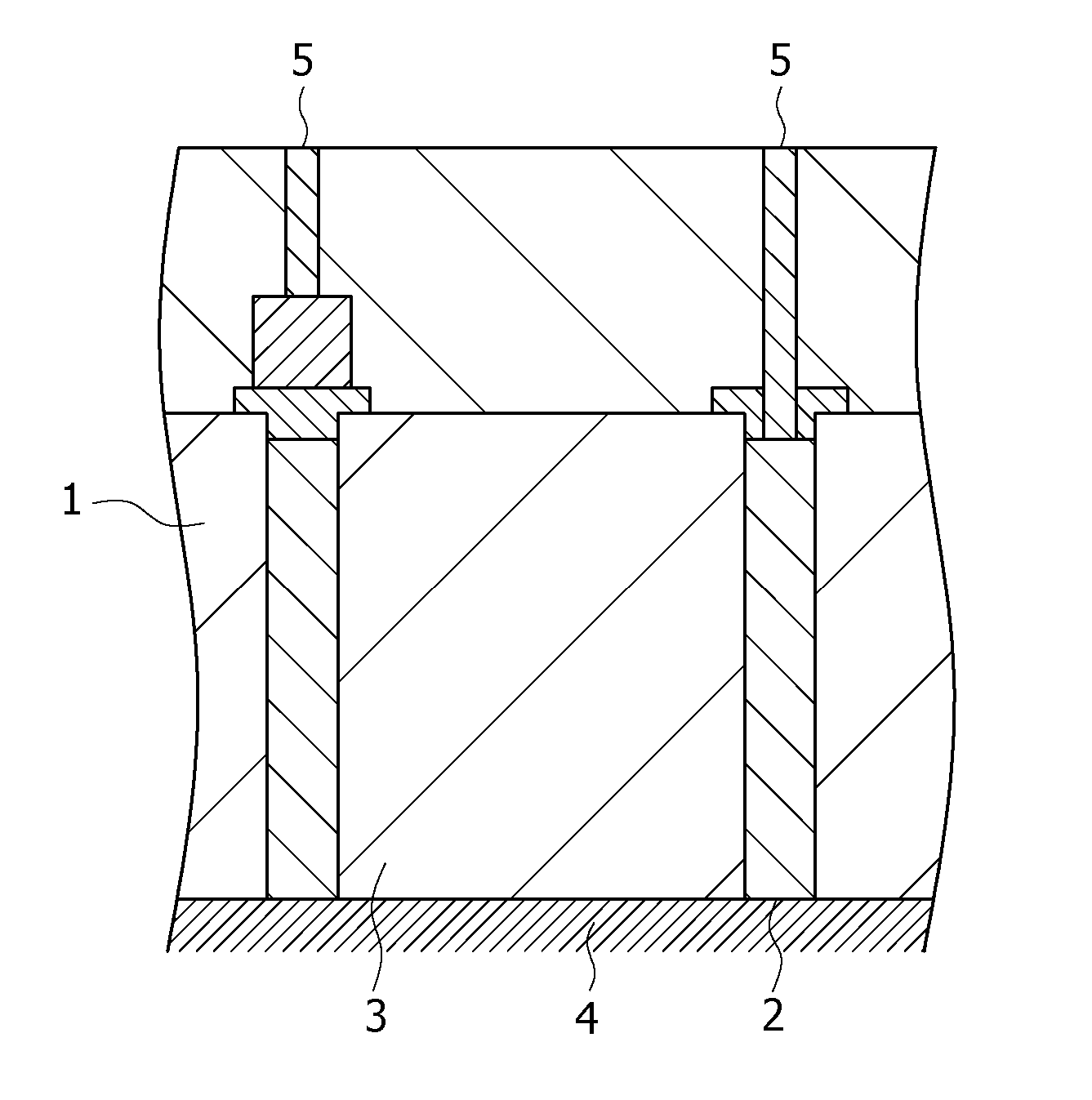
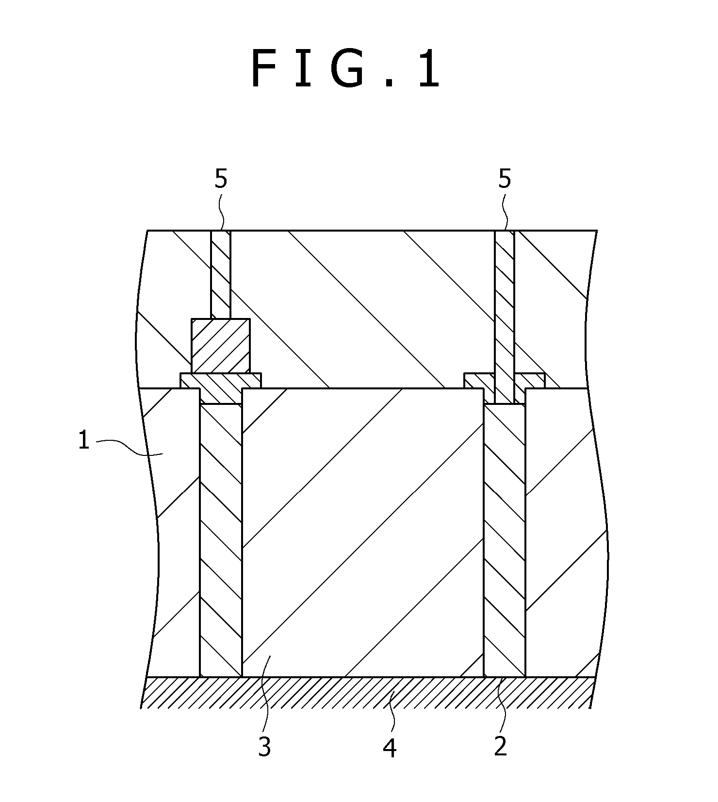
[0031]FIG. 1 is a schematic sectional view for illustrating an element isolation layer in a CMOS solid-state imaging device being an example of a solid-state imaging device to which the present invention is applied. In the CMOS solid-state imaging device herein shown, amorphous silicon containing B (boron) fills a trench-processed groove portion in an N-type silicon substrate 1 to form an element isolation layer 2. Furthermore, a light-receiving region 3 is formed in a region isolated by the element isolation layer, and also an overflow barrier region 4 is formed deep inside the N-type silicon substrate. Furthermore, an interconnection layer 5 is connected to the element isolation layer, and it is configured such that a negative voltage can be applied to the element isolation layer.

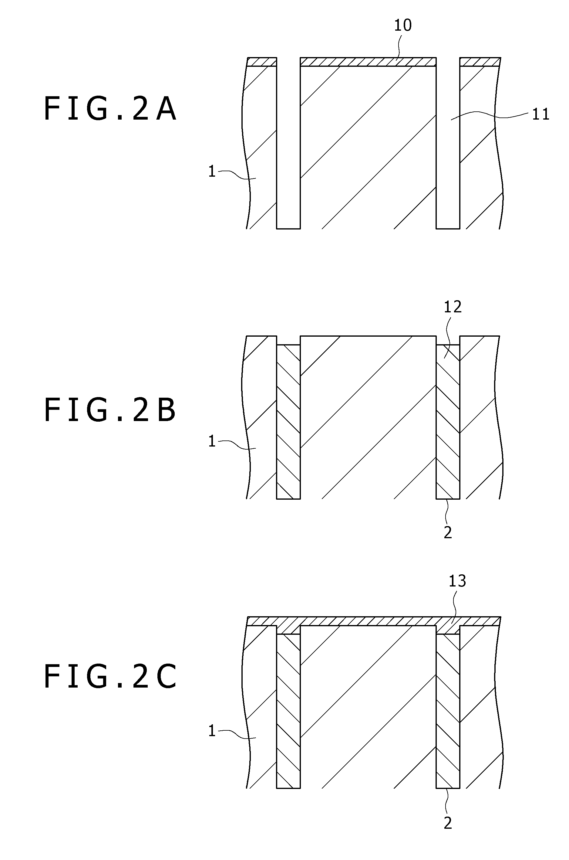
[0032] In FIG. 1, the trench structure on the left shows...


PUM


Abstract

The present invention provides a solid-state imaging device having an element isolation layer that is formed by embedding a conductive material into a trench-processed groove portion provided in a semiconductor base, in which a predetermined voltage is applied to the element isolation layer.

Description

CROSS REFERENCES TO RELATED APPLICATIONS [0001] The present invention contains subject matter related to Japanese Patent Application JP 2006-160001 filed in the Japanese Patent Office on Jun. 8, 2006, the entire contents of which being incorporated herein by reference. BACKGROUND OF THE INVENTION [0002] 1. Field of the Invention [0003] The present invention relates to a solid-state imaging device and a method of manufacturing the same. Particularly, the invention is directed to a solid-state imaging device having a structure in which a sensor portion extends to a deep position of a semiconductor base, and a method of manufacturing the same. [0004] 2. Description of Related Art [0005] Recently, along with a call for smaller, lighter and lower-power-consumption products using a solid-state imaging device, processing circuitry provided in a signal processing element has also been formed around a light-receiving portion of the solid-state imaging device, to allow all the processing to b...

Claims


Application Information

Patent Timeline
IPC IPC(8): H01L31/0224H01L31/18
CPCH01L27/14687Y02P70/50H01L27/1463H01L27/14689H01L27/14609H01L27/14643
Inventor WATANABE, SHINYA
Owner SONY CORP
Why Eureka
Try Eureka