Substrate dividing method

a substrate and dividing method technology, applied in the direction of manufacturing tools, welding/soldering/cutting articles, semiconductor/solid-state device details, etc., can solve the problems of side face chipping and cracking, and achieve the effect of preventing chipping and cracking and improving the transverse rupture strength of chips

Inactive Publication Date: 2008-04-17
HAMAMATSU PHOTONICS KK
View PDF99 Cites 134 Cited by
  • Summary
  • Abstract
  • Description
  • Claims
  • Application Information

AI Technical Summary

Benefits of technology

[0006] In view of such a circumstance, it is an object of the present invention to provide a substrate dividing method which can prevent chipping and cracking from occurring, and thin and divide a substrate.
[0009] In the step of grinding the substrate, the substrate is ground such that the substrate attains a predetermined thickness after the starting point region for cutting is formed within the substrate. Here, even when the ground surface reaches the fracture generated from the starting point region for cutting acting as a start point, cut surfaces of the substrate cut by the fracture remain in close contact with each other, whereby the substrate can be prevented from chipping and cracking upon grinding.
[0010] This can prevent chipping and cracking from occurring, and can thin and divide the substrate.
[0014] Preferably, the step of grinding the substrate includes a step of subjecting the rear face of the substrate to chemical etching. When the rear face of the substrate is subjected to chemical etching, the rear face of the substrate becomes smoother as a matter of course. Also, since the cut surfaces of the substrate cut by the fracture generated from the starting point region for cutting acting as a start point remain in close contact with each other, only edge parts on the rear face of the cut surfaces are selectively etched, so as to be chamfered. This can improve the transverse rupture strength of chips obtained by dividing the substrate, and prevent chipping and cracking from occurring in the chips.

Problems solved by technology

If the grinding of the rear face of the semiconductor substrate is performed by surface grinding in the methods described in the above-mentioned publications, however, chipping and cracking may occur at side faces of the groove formed beforehand in the semiconductor substrate when the surface-ground face reaches the groove.

Method used


Image

  • Substrate dividing method
  • Substrate dividing method
  • Substrate dividing method

Examples


example 1

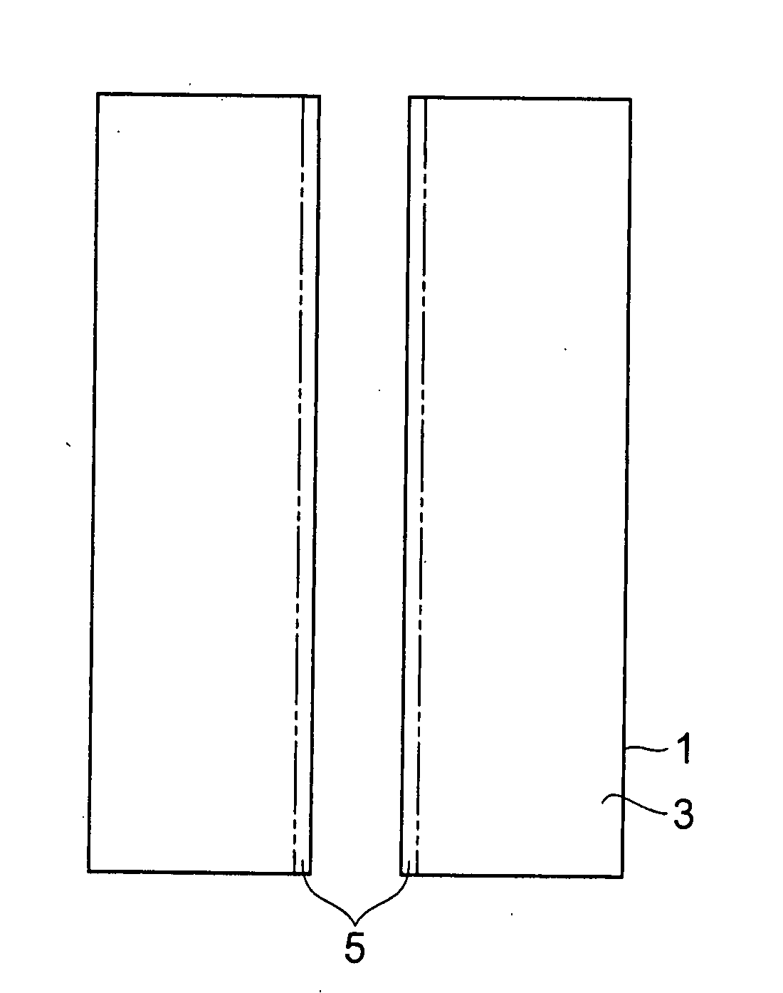
[0112] Example 1 of the substrate dividing method in accordance with the present invention will now be explained. Example 1 is directed to a case where the substrate 1 is a silicon wafer (having a thickness of 350 μm and an outer diameter of 4 inches) (“substrate 1” will hereinafter be referred to as “semiconductor substrate 1” in Example 1), whereas the front face 3 of the semiconductor substrate 1 is formed with a plurality of functional devices in a device manufacturing process.

[0113] First, before explaining a step of forming a starting point region for cutting within the semiconductor substrate 1, a laser processing apparatus employed in the step of forming a starting point region for cutting will be explained with reference to FIG. 14. FIG. 14 is a schematic diagram of the laser processing apparatus 100.

[0114] The laser processing apparatus 100 comprises a laser light source 101 for generating laser light L; a laser light source controller 102 for controlling the laser light...

example 2

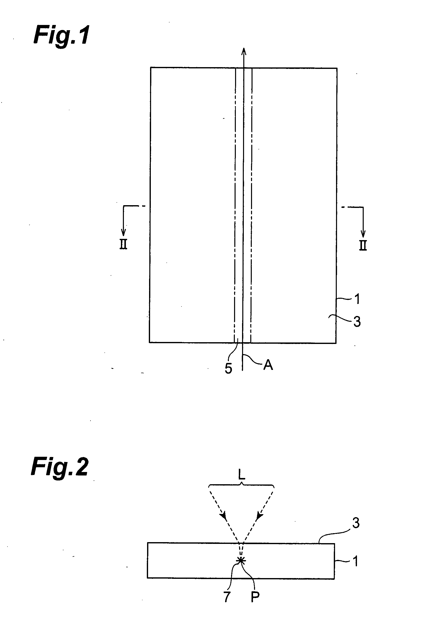
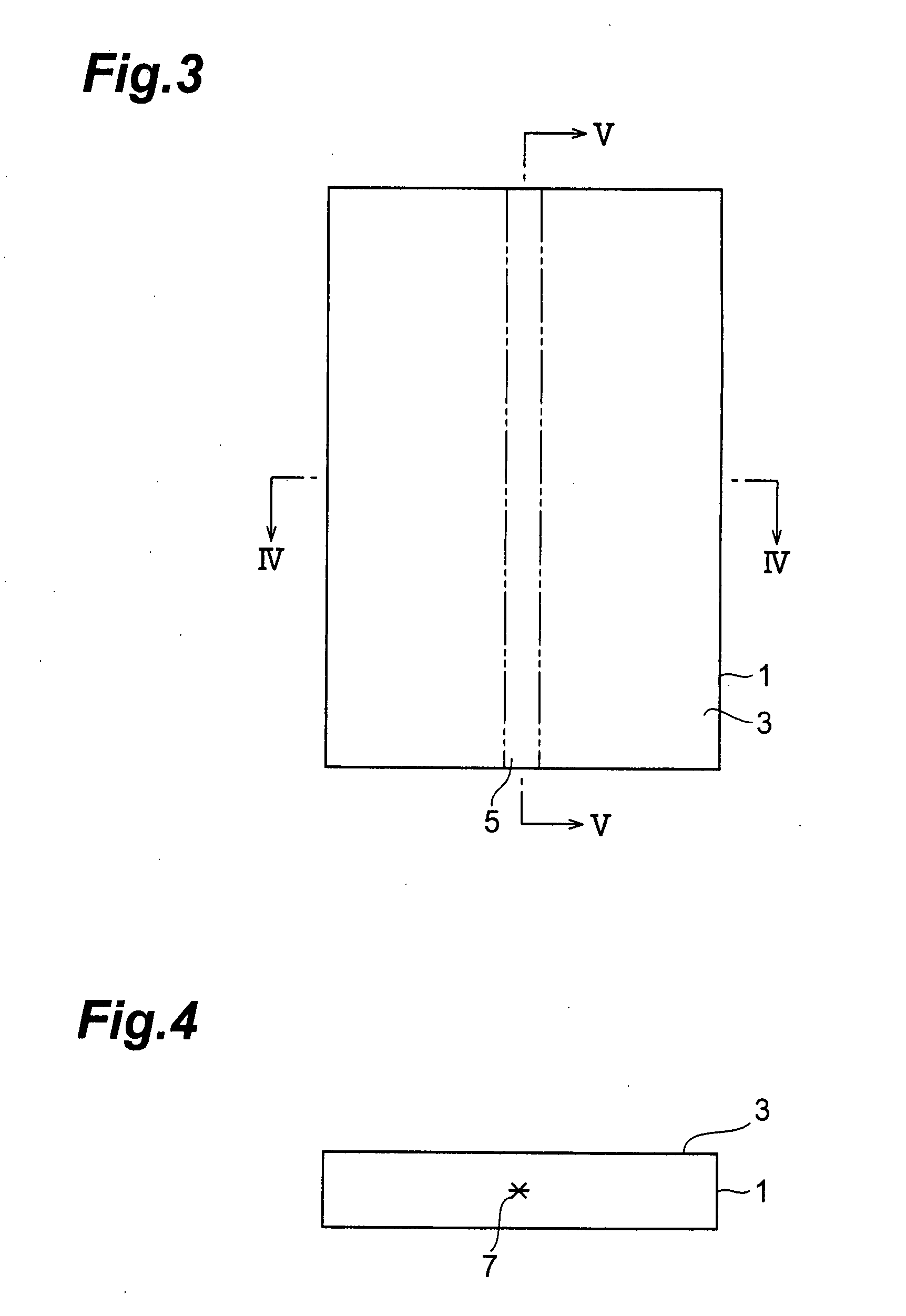
[0146] Example 2 of the substrate dividing method in accordance with the present invention will now be explained with reference to FIGS. 27 to 35. Example 2 relates to a case where the substrate 1 is a sapphire substrate (having a thickness of 450 μm and an outer diameter of 2 inches) which is an insulating substrate (“substrate 1” will hereinafter be referred to as “sapphire substrate 1” in Example 2), so as to yield a semiconductor chip to become a light-emitting diode. FIGS. 28 to 35 are sectional views of the sapphire substrate 1 taken along the line XX-XX of FIG. 27.

[0147] First, as shown in FIG. 28, the sapphire substrate 1 is irradiated with laser light L while a light-converging point P is positioned therewithin, so as to form a modified region 7 within the sapphire substrate 1. In a later step, a plurality of functional devices 19 are formed like a matrix on the front face 3 of the sapphire substrate 1, and the sapphire substrate 1 is divided into the functional devices 19...


PUM


Abstract

A substrate dividing method which can thin and divide a substrate while preventing chipping and cracking from occurring. This substrate dividing method comprises the steps of irradiating a semiconductor substrate 1 having a front face 3 formed with functional devices 19 with laser light while positioning a light-converging point within the substrate, so as to form a modified region including a molten processed region due to multiphoton absorption within the semiconductor substrate 1, and causing the modified region including the molten processed region to form a starting point region for cutting; and grinding a rear face 21 of the semiconductor substrate 1 after the step of forming the starting point region for cutting such that the semiconductor substrate 1 attains a predetermined thickness.

Description

TECHNICAL FIELD [0001] The present invention relates to a substrate dividing method used for dividing a substrate such as a semiconductor substrate in a step of making a semiconductor device or the like. BACKGROUND ART [0002] As semiconductor devices have been becoming smaller in recent years, there are cases where a semiconductor substrate is thinned to a thickness of several tens of micrometers in a step of making a semiconductor device. When thus thinned semiconductor substrate is cut and divided by a blade, chipping and cracking occur more than in the case where a semiconductor substrate is thicker, thereby causing a problem that the yield of semiconductor chips obtained by dividing the semiconductor substrate decreases. [0003] Known as semiconductor substrate dividing methods which can solve such a problem are those described in Japanese Patent Application Laid-Open Nos. SHO 64-38209 and SHO 62-4341. [0004] In the methods described in these publications, a semiconductor substra...

Claims


Application Information

Patent Timeline
Patent Type & Authority Applications(United States)
IPC IPC(8): H01L21/02B23K26/38B23K26/40B23K101/40H01L21/26H01L21/30H01L21/301H01L21/324H01L21/42H01L21/46H01L21/477H01L21/78H05K3/00
CPCB23K26/0057B23K26/063B23K26/4075B28D5/00H01L23/562H01L21/78H01L21/76894H01L21/304B28D5/0011H01L2924/0002B23K26/0622B23K26/40B23K26/53B23K2103/50H01L2924/00H01L21/268H01L21/6836H01L23/544H01L2221/68327H01L2223/5446H01L21/30604H01L2221/68336
Inventor FUJII, YOSHIMAROFUKUYO, FUMITSUGUFUKUMITSU, KENSHIUCHIYAMA, NAOKI
Owner HAMAMATSU PHOTONICS KK
Why Eureka
Try Eureka