Semiconductor structure and process for forming ohmic connections to a semiconductor structure

a semiconductor structure and semiconductor technology, applied in the field of semiconductor devices, can solve the problems of time and energy-consuming process, complicated and expensive implementation, etc., and achieve the effect of reducing the shading area of solar cells, and reducing the conversion efficiency of solar cells

Inactive Publication Date: 2008-04-24
DAY4 ENERGY
View PDF98 Cites 117 Cited by
  • Summary
  • Abstract
  • Description
  • Claims
  • Application Information

AI Technical Summary

Benefits of technology

[0020]In accordance with one aspect of the invention there is provided a semiconductor apparatus. The apparatus includes a first doped volume of semiconductor material, the first doped volume having a front surface and first and second adjacent regions. The first region has a first concentration of dopant and a first exposed area on the front surface. The second region has a second concentration of dopant and a second exposed area on the front surface, the second concentration being higher than the first concentration. The apparatus also includes a first external conductor and an alloy bonding the first external conductor to the second exposed area to ohmically connect the conductor to the second region.

Problems solved by technology

Generally the process is time and energy consuming, complicated, and may be expensive to implement, particularly for large area semiconductor devices such as photovoltaic cells.
This shading area decreases solar cell conversion efficiency.
Furthermore, diffusion of the contact metal into the front surface of the PV cell has a detrimental effect on charge recombination.
Bowing may be very pronounced on thin solar cells, which may be less than 180 micron thick, making such cells fragile thus reducing production yield.
The thin metal layer generally does not produce the bowing effect, even when used with very thin silicon wafers.
At the same time the need to use an additional coating of aluminum with an intermediate metallic layer in order to arrange reliable electrical contacting with electrical leads still appears to be a problem.
With thin film photovoltaic cells it is impossible to use technology that is conventional for crystalline silicon.
Unfortunately conductive pastes are expensive due to consumption of silver and have substantial electrical resistivity that is at least 10 times higher than copper wire.
It is known that PV solar cells experience substantial losses in the emitter region.
Although the use of a selective emitter has proved to be effective in improving PV solar cell efficiency, implementation of a selective emitter in practice, is quite complicated.
While this method allows fabricating a selective emitter and increased solar cell efficiency, it has a disadvantage in that selective emitter formation happens only after screen printed metallic patterns have been formed on the solar cell.
However, the proposed method requires that selective emitter formation be done only after screen printed metallization has been applied on the solar cell.

Method used


Image

  • Semiconductor structure and process for forming ohmic connections to a semiconductor structure
  • Semiconductor structure and process for forming ohmic connections to a semiconductor structure
  • Semiconductor structure and process for forming ohmic connections to a semiconductor structure

Examples


Embodiment Construction

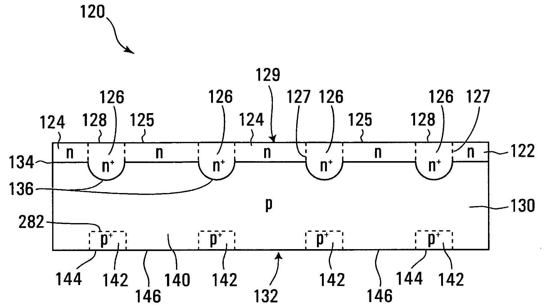
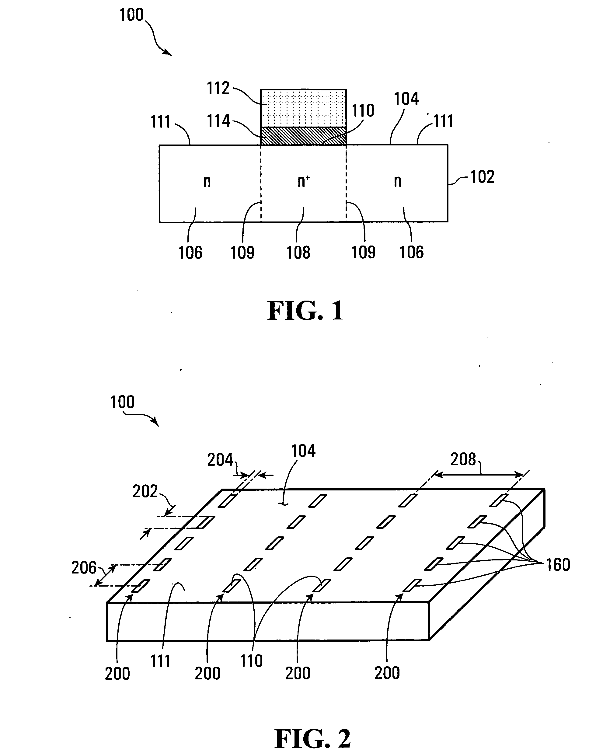
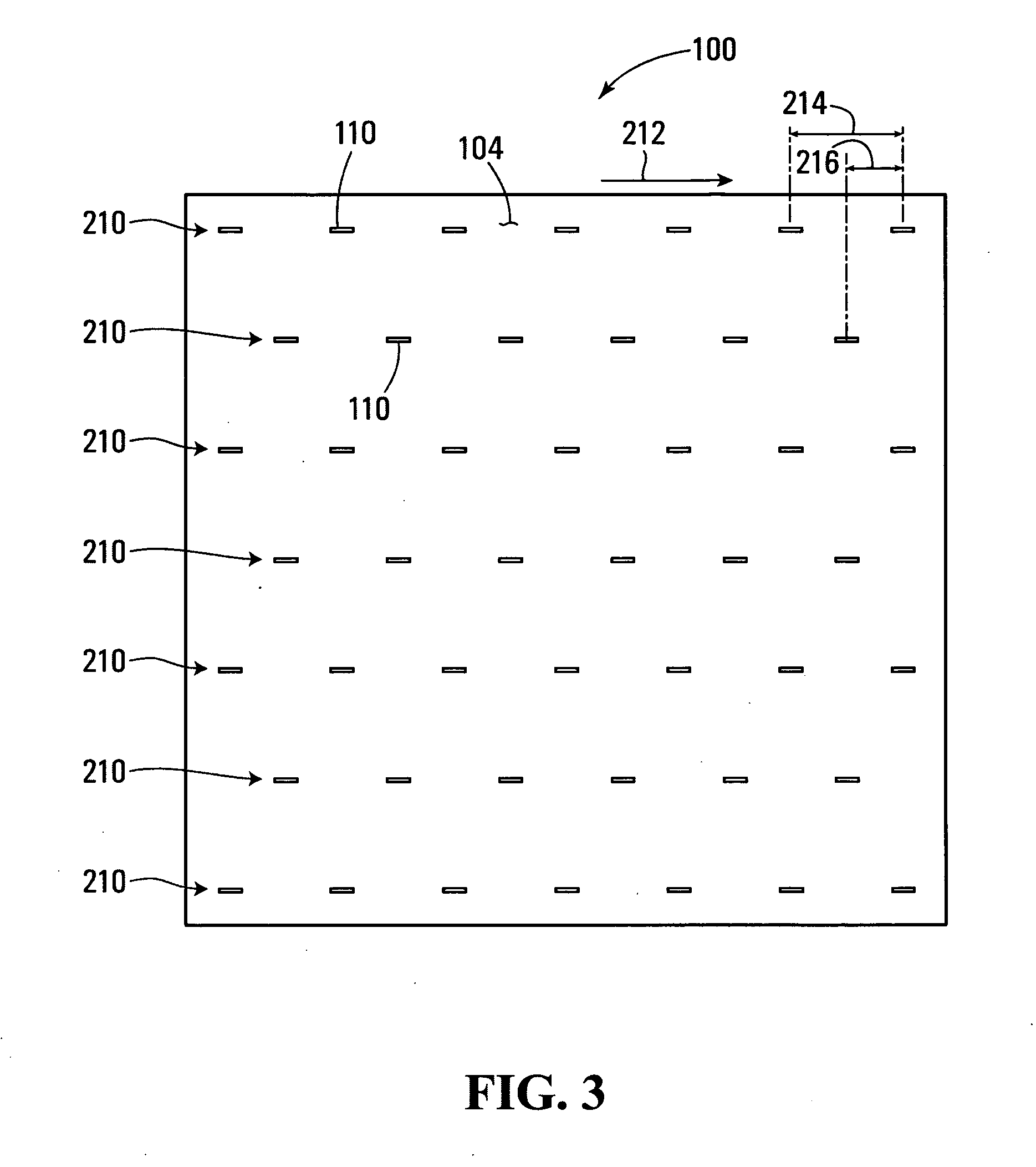
[0112]Referring to FIG. 1, a semiconductor apparatus in accordance with a first embodiment of the invention is shown generally at 100. The semiconductor apparatus 100 includes a first doped volume 102 of semiconductor material, having a front surface 104. The first doped volume 102 includes a first region 106 having a first concentration of dopant and a first exposed area 111 on the front surface 104. The first concentration of dopant causes the first region 106 to have a first polarity type such as n-type, for example. The first doped volume 102 also includes a second region 108 adjacent the first region 106. The second region 108 has a second concentration of the same dopant used to dope the first region 106 and has a second exposed area 110 on the front surface 104. The concentration of dopant in the second region 108 is higher than the concentration of dopant in the first region 106 and causes the second region 108 to have the same polarity type as the first region. Where n-type...


PUM


Abstract

A semiconductor apparatus is disclosed. The apparatus includes a first doped volume of semiconductor material, the first doped volume having a front surface and first and second adjacent regions. The first region has a first concentration of dopant and a first exposed area on the front surface. The second region has a second concentration of dopant and a second exposed area on the front surface, the second concentration being higher than the first concentration. The apparatus also includes a first external conductor and an alloy bonding the first external conductor to the second exposed area to ohmically connect the conductor to the second region.

Description

BACKGROUND OF THE INVENTION[0001]1. Field of Invention[0002]The present invention generally relates to semiconductor devices and more particularly to forming ohmic connections between external conductors and semiconductor devices.[0003]2. Description of Related Art[0004]Making ohmic contact to a semiconductor device typically involves deposition of a contact metal by screen printing, sputtering, evaporation, or chemical vapor deposition. The device is then generally annealed to cause the metal to at least partly diffuse into the semiconductor material to create an internal ohmic contact. Generally the process is time and energy consuming, complicated, and may be expensive to implement, particularly for large area semiconductor devices such as photovoltaic cells.[0005]Crystalline silicon photovoltaic (PV) cells are generally produced from a wafer having a p / n junction. The p / n junction may be produced by diffusion of either phosphorus or boron into a front side of a p-type or n-type ...

Claims


Application Information

Patent Timeline
Patent Type & Authority Applications(United States)
IPC IPC(8): H01L31/00
CPCY02E10/50H01L31/022425
Inventor RUBIN, LEONID
Owner DAY4 ENERGY
Why Eureka
Try Eureka