Method for treating the etching solution

a technology of etching solution and etching system, which is applied in the direction of decorative surface effects, electrical equipment, decorative arts, etc., can solve the problems of increasing the difficulty in controlling process parameters, affecting the stability of etching selectivity, and affecting the quality of etching, so as to reduce the cost of the etching process and stable etching selectivity

US20080093343A1Inactive Publication Date: 2008-04-24PROMOS TECH INC
2 Cites 2 Cited by

Patent Information

Authority / Receiving Office
US · United States
Patent Type
Applications(United States)
Current Assignee / Owner
Publication Date
2008-04-24
Estimated Expiration
Not applicable · inactive patent

Smart Images

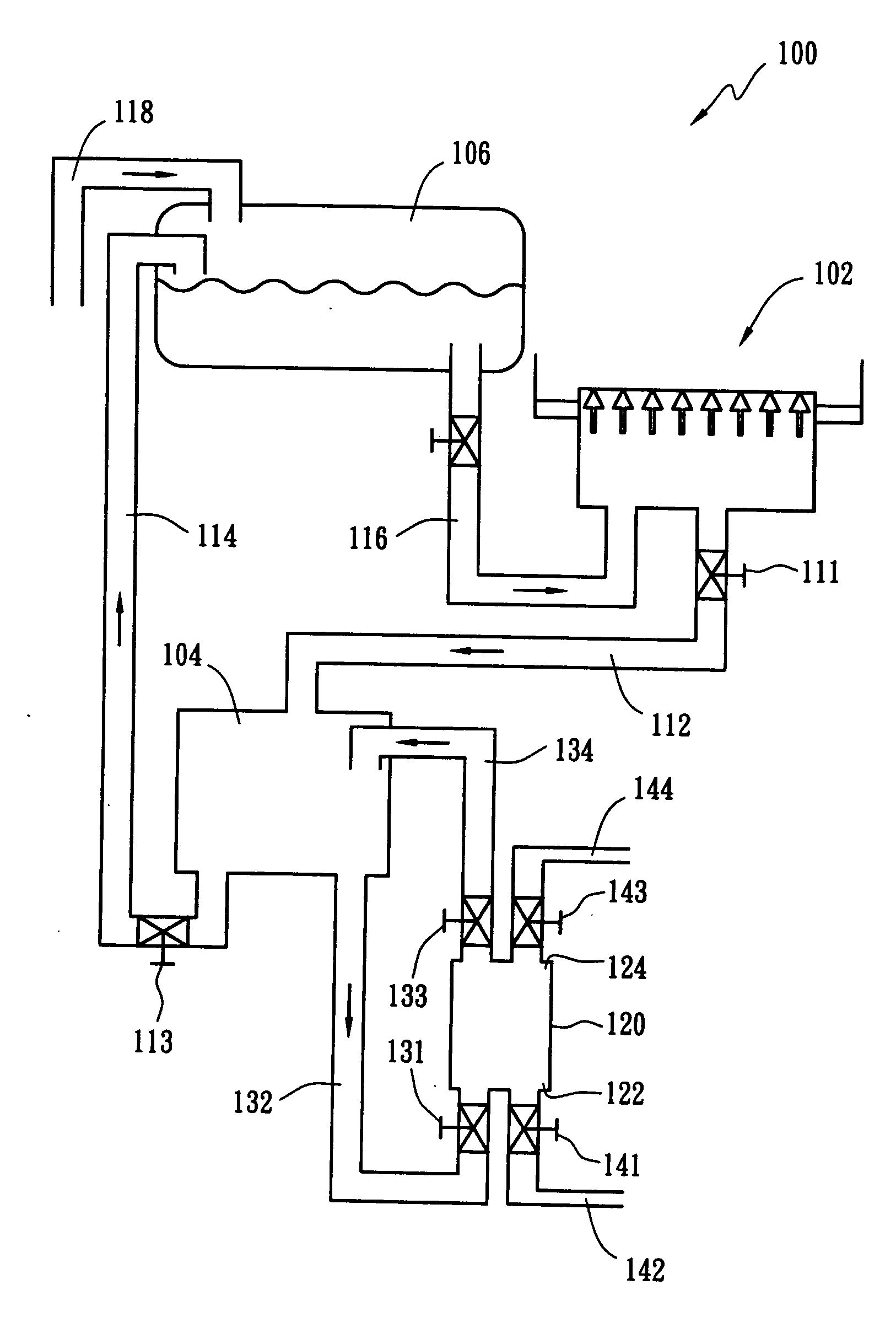
  • Figure 1
    Figure 1
  • Figure 2
    Figure 2
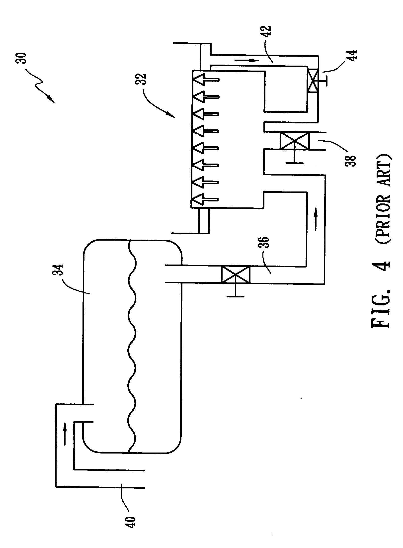
  • Figure 3
    Figure 3
Patent Text Reader

Abstract

The present etching system includes a processing tank with an etching solution containing silicon, a cooling tank, a pre-heating tank, a first pipe for transferring the etching solution from the processing tank to the cooling tank, a second pipe for transferring the etching solution from the cooling tank to the pre-heating tank, and a third pipe for transferring the etching solution from the pre-heating tank to the processing tank. The present method for treating the etching solution first performs an etching process using the etching solution, which is then cooled to a first temperature to form a silicon-saturated etching solution. After silicon-containing particles larger than a predetermined size are filtered out, the silicon-saturated etching solution is heated to a second temperature to form a non-saturated etching solution for performing another etching process later. The second temperature is preferably at least 10° C. higher than the first temperature.
Need to check novelty before this filing date? Find Prior Art

Description

[0001] This is a Continuation of application Ser. No. 11 / 535,057 filed Sep. 25, 2006, which in turn is a Divisional of application Ser. No. 10 / 943,936. The disclosure of the prior applications is hereby incorporated by reference herein in its entirety.BACKGROUND

[0002] (A) Field of the Invention

[0003] The present invention relates to an etching system and method for treating the etching solution thereof, and more particularly, to an etching system and a method for treating the etching solution with a stable selectivity between silicon nitride and silicon oxide.

[0004] (B) Description of the Related Art

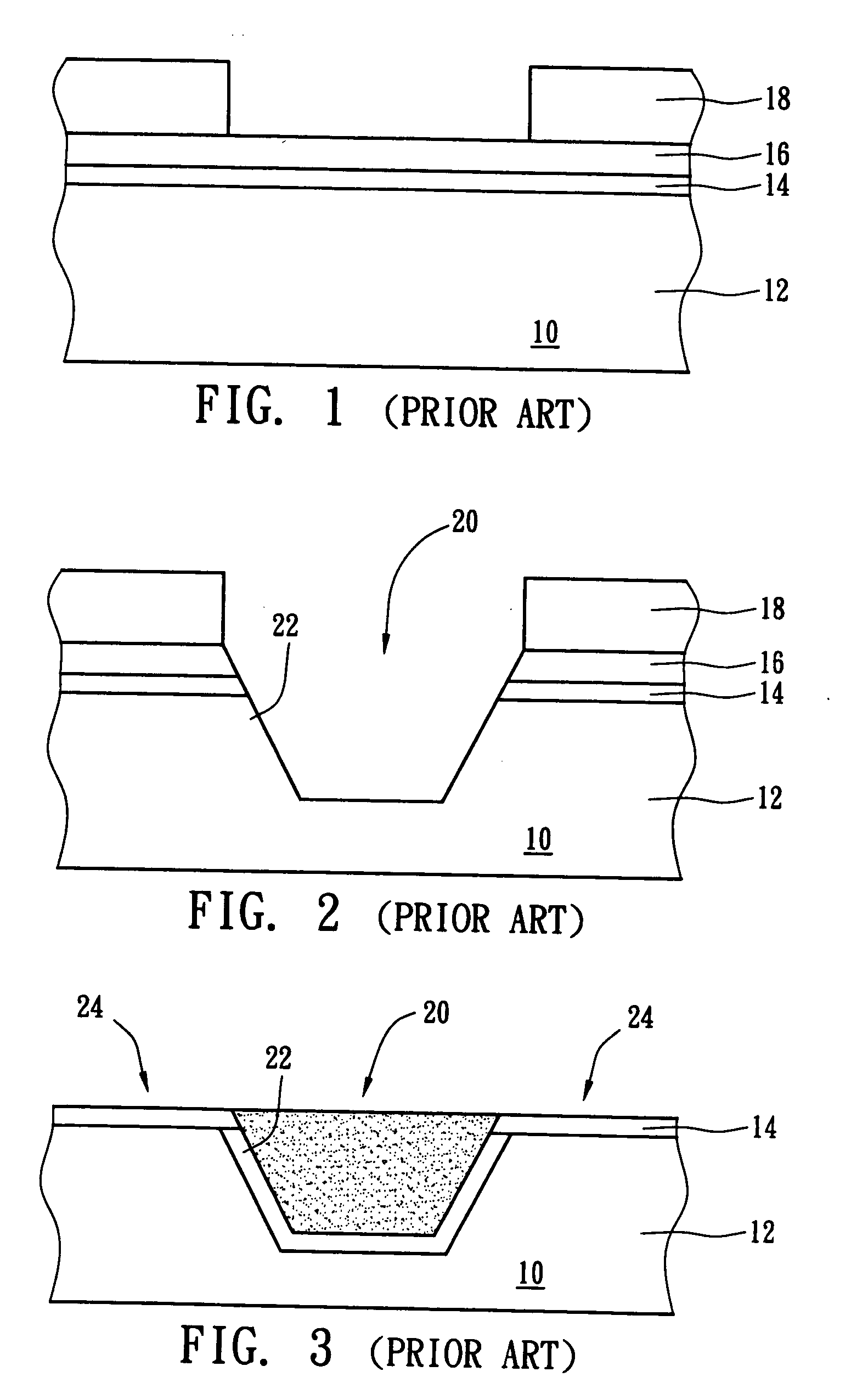
[0005] FIG. 1 to FIG. 3 show a method for fabricating a shallow trench isolation on a wafer 10 according to the prior art. The shallow trench isolation is widely used in the fabrication of the metal-oxide-semiconductor (MOS) transistor to form an electrical isolation between transistors. As shown in FIG. 1, the fabrication of the shallow trench isolation begins to form an oxide layer ...

Examples

Embodiment Construction

[0027]FIG. 7 shows the relation between the silicon concentration and both the etching rate and silicon particle concentration in the etching solution. Curve 72 represents the etching curve of silicon nitride, curve 74 represents the etching curve of silicon oxide, and curve 76 is a variation curve of the silicon particle concentration. As shown in FIG. 7, the etching rate of silicon nitride is substantially not influenced by the silicon concentration virtually and is fixed at about 90 Å / min. In contrary, the etching rate of silicon oxide reduces as the silicon concentration increases, and is fixed at about 0.2 Å / min as the silicon concentration is above 100 ppm. When the silicon concentration is above 100 ppm, the silicon particle concentration of the etching solution increases as the silicon concentration increases.

[0028]FIG. 8 shows the relation between the silicon saturation concentration of the etching solution (i.e. the solubility of silicon in the etching solution) and the t...