Metal-oxide-semiconductor device having trenched diffusion region and method of forming same

a technology of metal-oxidesemiconductor and diffusion region, which is applied in the direction of semiconductor devices, electrical equipment, transistors, etc., can solve the problems of not significantly increasing the cost of manufacturing ic devices, and achieve the effects of reducing the on-state resistance of mos devices, increasing output capacitance, and improving high-frequency performance and dc performance of devices

Active Publication Date: 2008-04-24
BELL SEMICON LLC
View PDF3 Cites 17 Cited by
  • Summary
  • Abstract
  • Description
  • Claims
  • Application Information

AI Technical Summary

Benefits of technology

[0007] The present invention provides techniques for reducing the on-state resistance of an MOS device without significantly increasing output capacitance in the device, thereby improving high-frequency performance and DC performance of the device. Moreover, the techniques of the present invention can be used to fabricate an IC device, for example, an LDMOS device, using conventional CMOS-compatible process technology. Consequently, the cost of manufacturing the IC device is not significantly increased.
[0009] The given source / drain region may include a plurality of trenches formed in the semiconductor layer proximate the upper surface of the semiconductor layer. A spacing of the trenches is arranged such that a wall separating two adjacent trenches is comprised substantially entirely of material of the second conductivity type. In this manner, a junction capacitance associated with the MOS device is substantially independent of a depth of the trenches, and instead is a function of a linear width of the given source / drain region. An on-state resistance in the MOS device is therefore advantageously reduced without any significant increase in the junction capacitance of the device.

Problems solved by technology

Consequently, the cost of manufacturing the IC device is not significantly increased.

Method used


Image

  • Metal-oxide-semiconductor device having trenched diffusion region and method of forming same
  • Metal-oxide-semiconductor device having trenched diffusion region and method of forming same
  • Metal-oxide-semiconductor device having trenched diffusion region and method of forming same

Examples


third embodiment

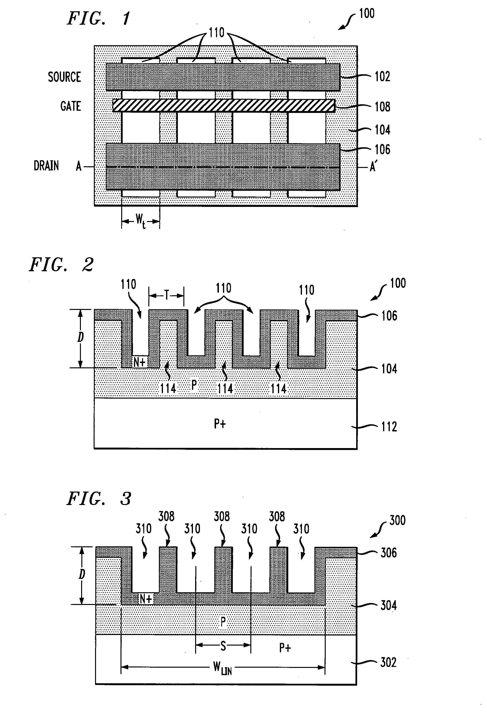
[0040]FIG. 5 is a cross-sectional view depicting at least a portion of an exemplary MOS device 500, formed in accordance with the invention. In the figure, a cross section of a drain region 506 in the MOS device 500 is primarily shown. The MOS device 500 preferably includes a P-type epitaxial layer 504 formed on a P+ substrate 502. Like the MOS device 300 shown in FIG. 3, the MOS device 500 includes a plurality of trenches 510 formed in the epitaxial layer 504 proximate an upper surface of the epitaxial layer. In comparison to the trenches 310 in the MOS device 300 of FIG. 3, trenches 510 of MOS device 500 are preferably formed having undercut sidewalls 514, such that a bottom wall of a given trench is wider than an upper opening of the trench. Undercut sidewalls may be formed, for example, by using an anisotropic etching process. In this manner, trenches 510 having sidewalls of a desired slope (e.g., a positive and / or a negative slope) can be formed.

[0041] Preferably, a spacing bet...

fourth embodiment

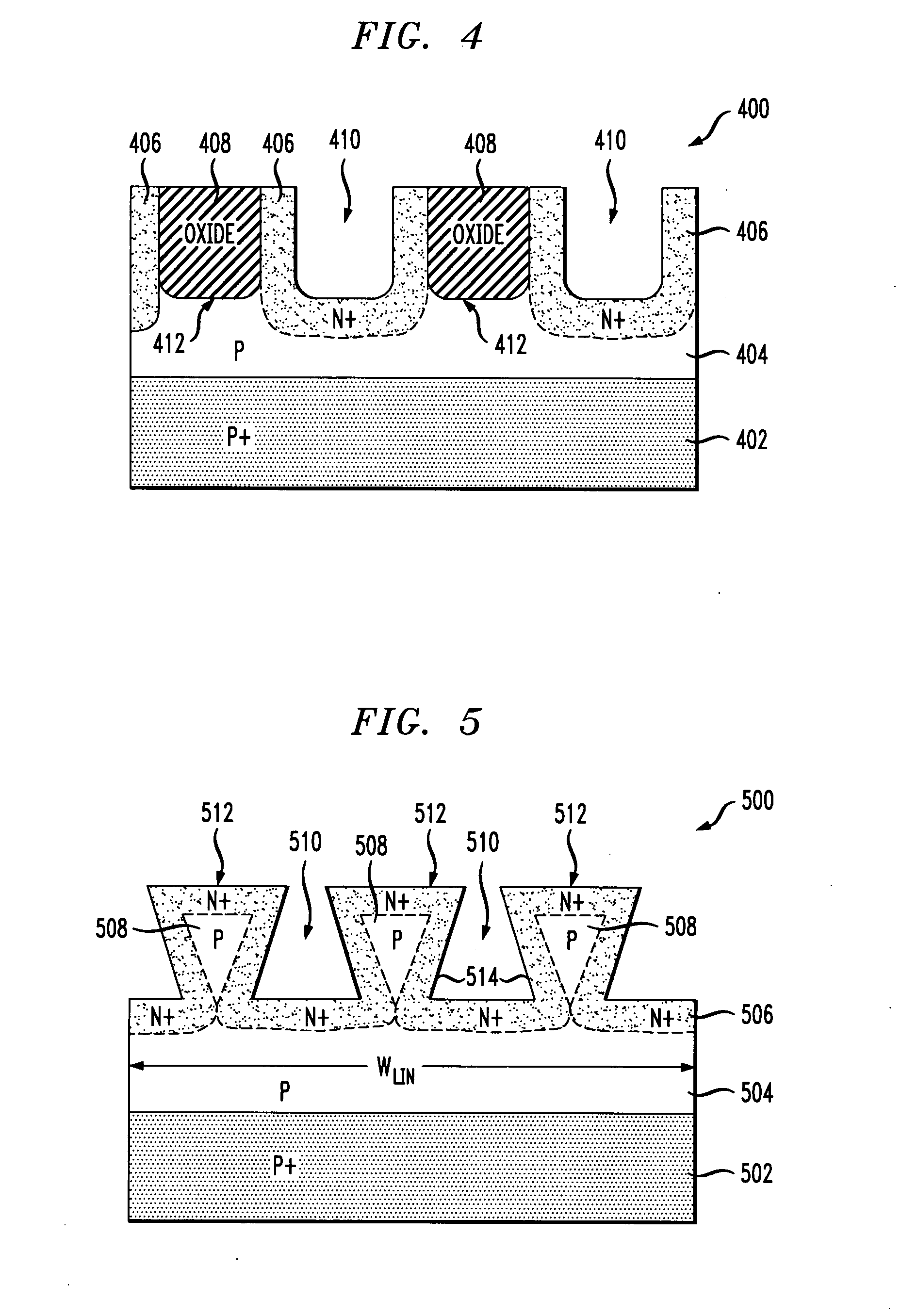
[0043]FIG. 6 is a cross-sectional view illustrating at least a portion of an exemplary MOS device 600, formed in accordance with the invention. The figure primarily illustrates a drain region 606 in the MOS device 600. Like the illustrative MOS device embodiments previously described in conjunction with FIGS. 3-5, the exemplary MOS device 600 is advantageously configured such that an effective width Weff of a channel region in the device is substantially greater than a width of a P-N junction in the device. This enables an electrical conductance of the MOS device 600 to be beneficially increased, thereby reducing on-state resistance, without any significant increase injunction capacitance in the device.

[0044] The MOS device 600 preferably includes a P-type epitaxial layer 604 formed on a P+ substrate 602. A plurality of trenches 610 are formed in the epitaxial layer 604 proximate an upper surface of the epitaxial layer. Mesas 612 formed between adjacent trenches 610 are preferably c...


PUM


Abstract

An MOS device includes a semiconductor layer of a first conductivity type and first and second source / drain regions of a second conductivity type formed in the semiconductor layer proximate an upper surface of the semiconductor layer. The first and second source / drain regions are spaced apart relative to one another. A gate is formed above and electrically isolated from the semiconductor layer, at least partially between the first and second source / drain regions. At least a given one of the first and second source / drain regions is configured having an effective width that is substantially greater than a width of a junction between the semiconductor layer and the given source / drain region.

Description

CROSS-REFERENCE TO RELATED APPLICATION(S) [0001] This application is a divisional of pending U.S. application Ser. No. 10 / 953,018 filed on Sep. 29, 2004, the disclosure of which is incorporated by reference herein.FIELD OF THE INVENTION [0002] The present invention relates generally to semiconductor devices, and more particularly relates to a metal-oxide-semiconductor (MOS) device having improved high-frequency performance and a method of forming same. BACKGROUND OF THE INVENTION [0003] MOS devices, including laterally diffused MOS (LDMOS) devices, are employed in a variety of applications, such as, for example, power amplifiers in wireless communications systems. With regard to the direct current (DC) performance of LDMOS devices, it is generally desirable to have a low on-state resistance and a high transconductance. The on-state resistance of a low-voltage (e.g., breakdown voltage of less than about 10 volts) LDMOS device is dominated primarily by a resistance in a channel region...

Claims


Application Information

Patent Timeline
Patent Type & Authority Applications(United States)
IPC IPC(8): H01L29/78H01L21/336
CPCH01L21/223H01L21/2253H01L21/266H01L29/0653H01L29/0657H01L29/7835H01L29/0886H01L29/1037H01L29/66659H01L29/66681H01L29/7816H01L29/0847H01L29/0852
Inventor SHIBIB, MUHAMMED AYMANXU, SHUMING
Owner BELL SEMICON LLC
Why Eureka
Try Eureka