Continuously Referencing Signals over Multiple Layers in Laminate Packages

a signal and laminate technology, applied in the direction of high frequency circuit adaptation, sustainable manufacturing/processing, final product manufacturing, etc., can solve the problems of degrading the signal being transmitted, unable to provide more and more input/output (i/o) interconnections to chips that are shrinking in size and growing in complexity, and unable to meet the needs of increasing the number of chips, so as to avoid discontinuities in voltage reference.

Inactive Publication Date: 2008-04-24
GLOBALFOUNDRIES INC
View PDF1 Cites 38 Cited by
  • Summary
  • Abstract
  • Description
  • Claims
  • Application Information

AI Technical Summary

Benefits of technology

[0020]In one exemplary embodiment, a source voltage plane is connected from the first layer in the first area to one of the two intermediate layers in the second area using one or more vias. In a further exemplary embodiment, the conductive signal plane is connected from a second layer within two intermediate layers in the first area to a third layer within the two intermediate layers in the second area using one or more vias. In a still further exemplary embodiment, a ground plane is connected from the third layer in the first area to the fourth layer in the second area using one or more vias such that the signal plane maintains a balanced proximity to the source voltage plane and the ground plane.

Problems solved by technology

Creating a mounting for a chip might seem trivial to the uninitiated, but the ability to provide more and more input / output (I / O) interconnections to chips that are shrinking in size and growing in complexity is an ever-present problem.
With a lossy transmission line model, there may be reflections from characteristic impedance changes, which degrade the signal being transmitted.
In addition, even though having the source voltage plane on top may provide ideal voltage referencing in an area under a particular chip, having the source voltage plane on top may cause reliability issues in areas away from the chip.
This would result in a break in the voltage reference.
That is, due to the chip design and the chosen top layer, the signal layer may pass under holes in the top layer, and in these areas the signal path may not have ideal transmission line characteristics.
This design may attempt to provide an ideal voltage reference for all areas of the package; however, the signal plane may cross a void where the voltage reference switches or breaks, which causes distortion and degrades the quality of the signal at the receiving end.

Method used


Image

  • Continuously Referencing Signals over Multiple Layers in Laminate Packages
  • Continuously Referencing Signals over Multiple Layers in Laminate Packages
  • Continuously Referencing Signals over Multiple Layers in Laminate Packages

Examples


Embodiment Construction

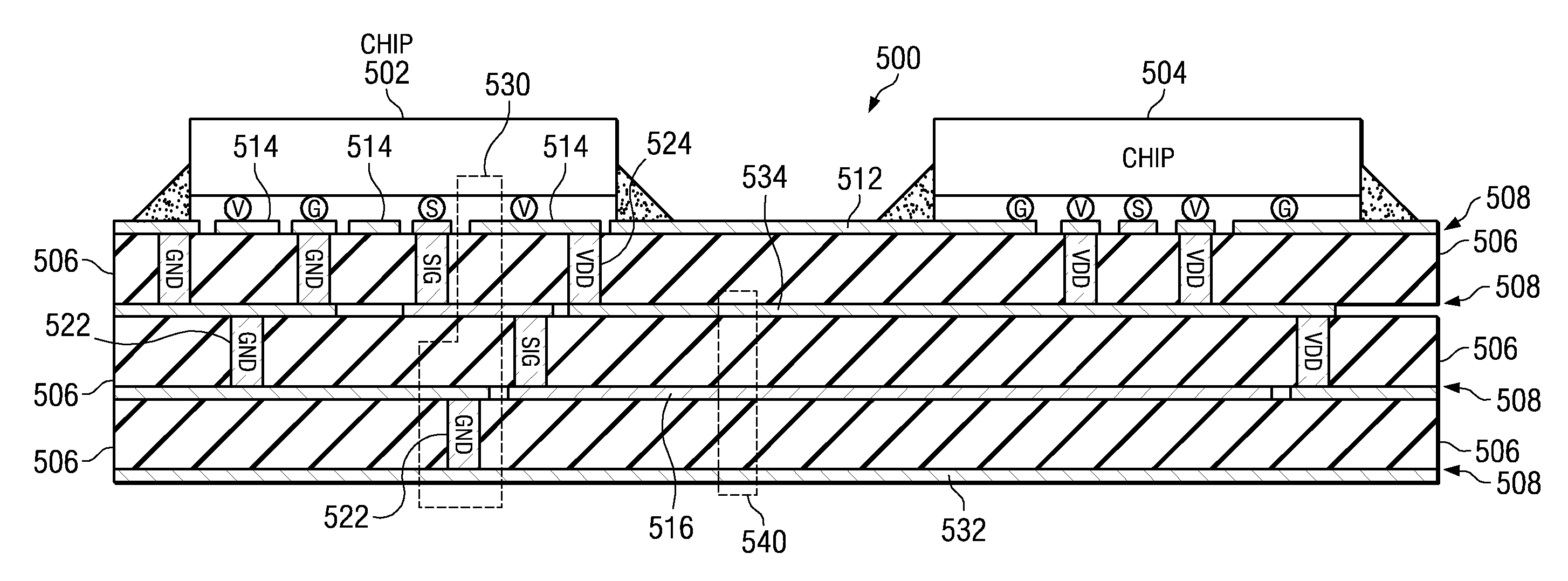
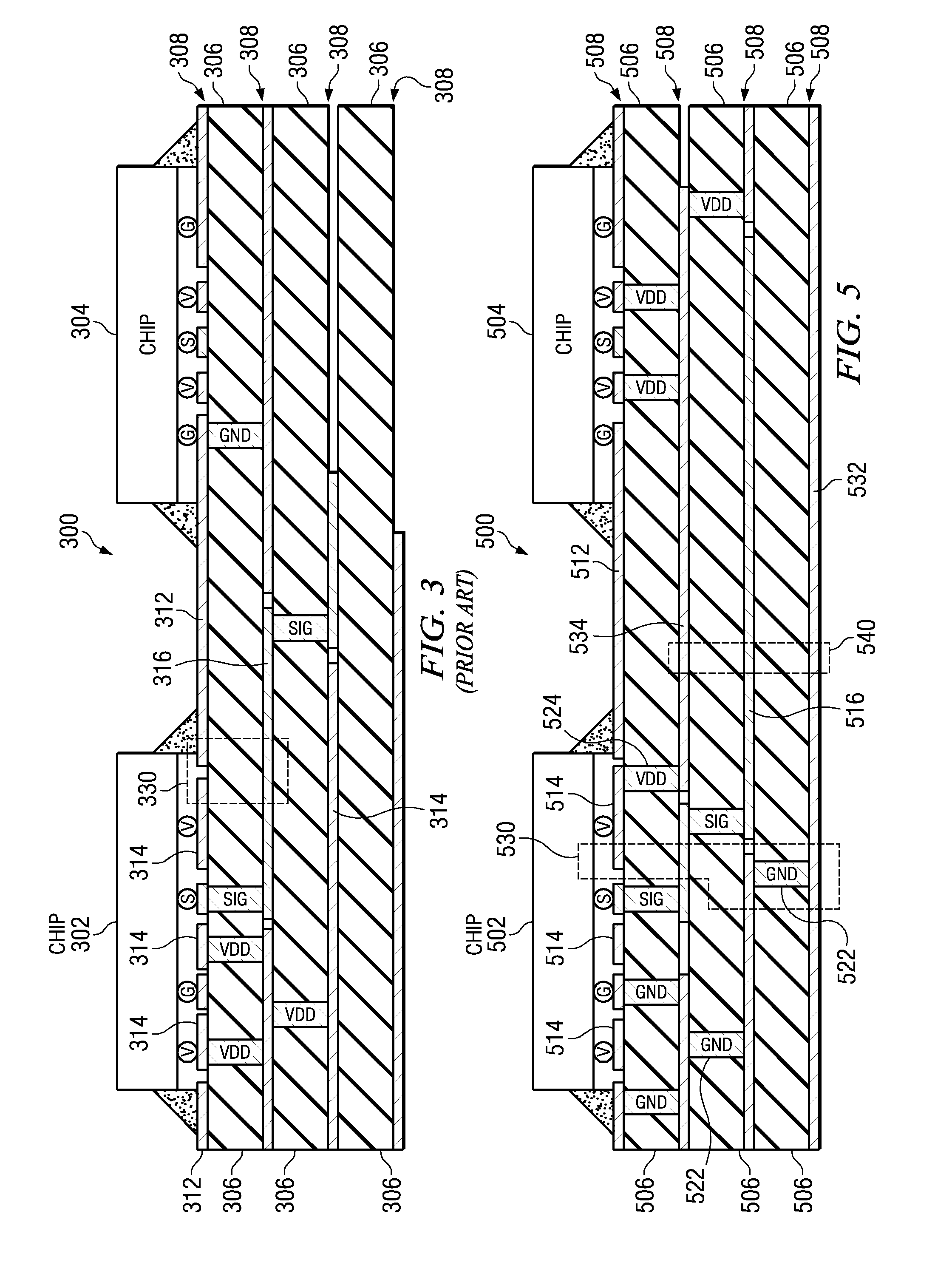
[0040]The illustrative embodiments provide an improved mechanism for continuously referencing signals over multiple layers in laminate packages. In order to illustrate the primary configuration differences between the improved package design configuration and known laminate packages, reference will first be made to FIGS. 1-4, which illustrate various views of known package designs.

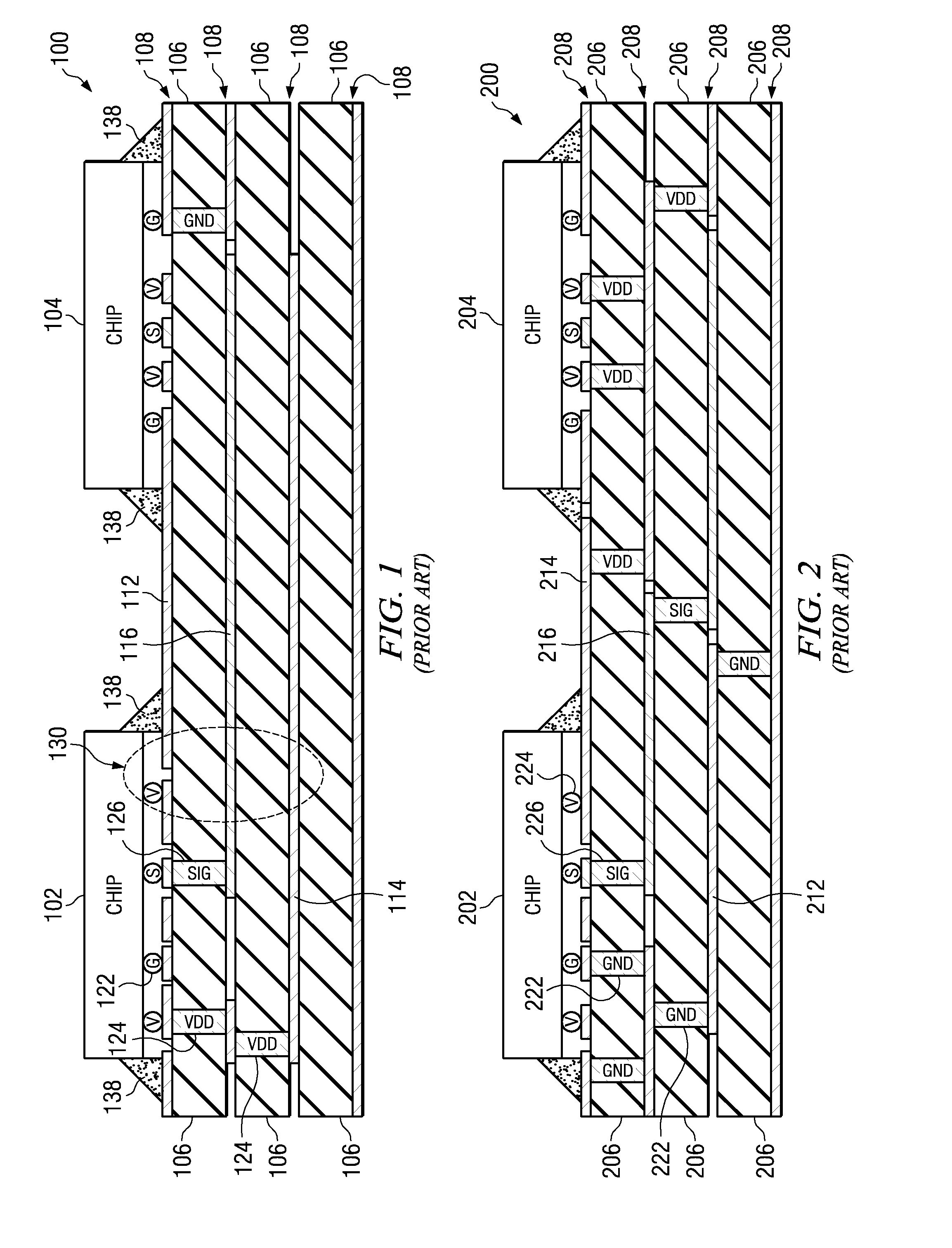
[0041]FIG. 1 illustrates an example cross-section of a chip package with a ground voltage, or potential, plane on top. The package includes chip 102 and chip 104, which are placed on package 100. Package 100 comprises a plurality of insulator layers 106 and a plurality of patterned conductor layers 108. Package 100 may also be referred to as a “chip carrier” or “substrate.” Chips 102, 104 may be sealed to the package substrate using hermetic seal 138, for example.

[0042]In the example depicted in FIG. 1, ground voltage plane 112 is the top voltage plane. Chip 102 may be connected to ground (GND) plane 112 u...


PUM


Abstract

A mechanism for continuously referencing signals over multiple layers in laminate packages provides a continuous path for signals from one layer to another while using the ideal voltage reference for all areas of the package and still avoiding discontinuities in the voltage reference. A reference plane adjustment engine analyzes a package design and identifies an ideal top plane for all areas of the package, including areas under particular chip die(s) and areas that are not under a chip die. The reference plane adjustment engine then modifies the package design to reposition ground planes, source voltage planes, signal planes, and vias between layers to maintain a continuous voltage reference regardless of the top layer. The reference plane adjustment engine provides the resulting mixed voltage plane package design to a design analysis engine. A package fabrication system fabricates the package.

Description

BACKGROUND[0001]1. Technical Field[0002]The present application relates generally to an improved package design configuration. More specifically, the present application is directed to a method and apparatus for continuously referencing signals over multiple layers in laminate packages.[0003]2. Description of Related Art[0004]A die is an unpackaged piece of silicon containing the functional components of a device. “Die,” also referred to as a “chip” herein, is the formal term for the piece of silicon containing an integrated circuit. A package is a housing that chips come in for plugging into or soldering onto printed circuit boards. The package provides electrical wiring and connections to pins. A lid covers the chip and bonds with the package.[0005]The exemplary aspects of the present invention concern an improved package design configuration with continuous voltage reference for signals transmitted through layers of a laminate package. A discussion of laminate packages follows to...

Claims


Application Information

Patent Timeline
Patent Type & Authority Applications(United States)
IPC IPC(8): H01L23/12
CPCH01L23/50H01L23/5383H01L2224/73204H01L2224/32225H01L2224/16225H01L2924/01004H01L2924/01079H01L2924/09701H01L2924/3011H01L2924/3025H05K1/0253H05K1/0298H05K1/181H05K2201/09336H05K2201/09345H05K2201/10522H05K2201/10674H01L2924/00H01L2924/00014H01L2924/00011Y02P70/50H01L2224/0401
Inventor PREDA, FRANCESCOWALLS, LLOYD A.
Owner GLOBALFOUNDRIES INC
Why Eureka
Try Eureka