Regulated analog switch

a technology of analog switch and regulated switch, applied in the direction of regulating electric variables, preventing network interference, instruments, etc., can solve problems such as affecting the operation of the switch, and achieve the effect of reducing the on-resistan

Active Publication Date: 2008-04-24
DIALOG SEMICONDUCTOR GMBH
View PDF4 Cites 6 Cited by
  • Summary
  • Abstract
  • Description
  • Claims
  • Application Information

AI Technical Summary

Benefits of technology

[0014]A further object of the present invention is to achieve methods and circuits for a regulated analog switch having an output voltage not exceeding a defined voltage limit, wherein the input voltage could be much higher than the defined output voltage.
[0015]Another object of the present invention is to achieve methods and circuits for a regulated analog switch having an output voltage not exceeding a defined voltage limit, wherein the input voltage could be higher than 12 Volts.
[0016]Another object of the present invention is to achieve methods and circuits for a regulated analog switch having an output voltage not exceeding a defined voltage limit, wherein the output current is constant over a variable input voltage ranging between a order of magnitude of 5 Volts and an order of magnitude of more than 40 Volts.
[0017]In accordance with the objects of this invention a method for a regulated analog switch providing a constant output voltage not exceeding a defined voltage limit, wherein an input voltage could be much higher than this defined output voltage limit and wherein the ON-resistance of the switch can be reduced to a minimum, has been achieved. The method invented comprises, first, to provide a supply voltage smaller than the maximum extended drain voltage of said transistor switch, said transistor switch, a voltage divider between said output voltage and ground, a differential amplifying means having its output connected to the gate of said high voltage transistor, a reference voltage being lower than said supply voltage, and a resistive means connected between said supply voltage and the gate of said transistor switch. The following steps comprise to bias said differential amplifying means with said supply voltage, to amplify the difference between the midpoint voltage of said voltage divider and said reference voltage and using the amplified difference to control the gate of said high-voltage transistor, and to minimize the ON-resistance of said high voltage transistor by applying a maximal allowable gate-source voltage to said transistor in case said supply voltage is smaller or equal than said defined output voltage. The last step of the method comprises to clip the output voltage by adjusting said reference voltage and said voltage divider.
[0018]In accordance with the objects of this invention a circuit for a regulated analog MOSFET switch providing a constant output voltage not exceeding a defined voltage limit, wherein an input voltage could be much higher than this defined output voltage limit and wherein the ON-resistance of the switch can be reduced to a minimum, has been achieved, The circuit invented is comprising, first, a supply voltage being smaller than the maximum extended drain voltage of said MOSFET switch, a reference voltage being lower than said supply voltage, and a MOSFET transistor used as switch being connected between said supply voltage and said output voltage, wherein its gate is connected to a second terminal of a resistive means and to an output of ...

Problems solved by technology

All of these switches are limited on what signals they can pass/stop by their gate to source, gate to drain and source to drain voltages, at which time the FETs are damaged.
It is a challenge for the...

Method used


Image

  • Regulated analog switch
  • Regulated analog switch
  • Regulated analog switch

Examples


Embodiment Construction

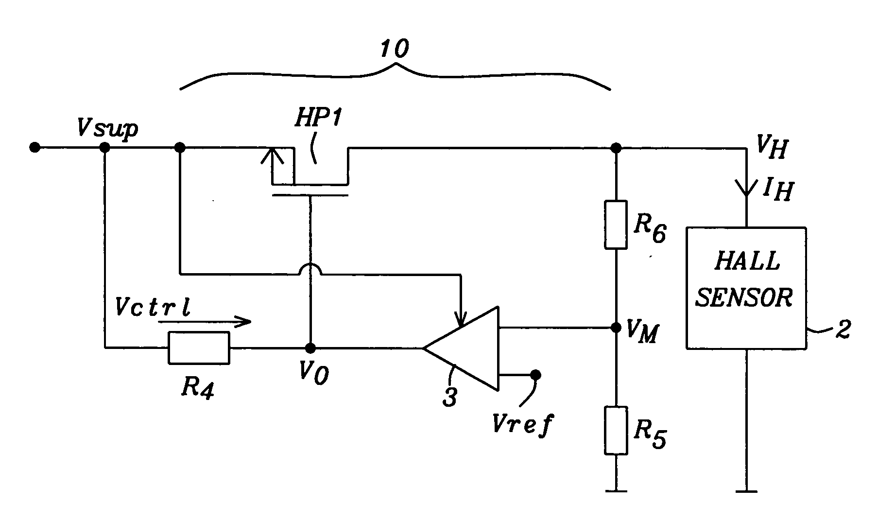
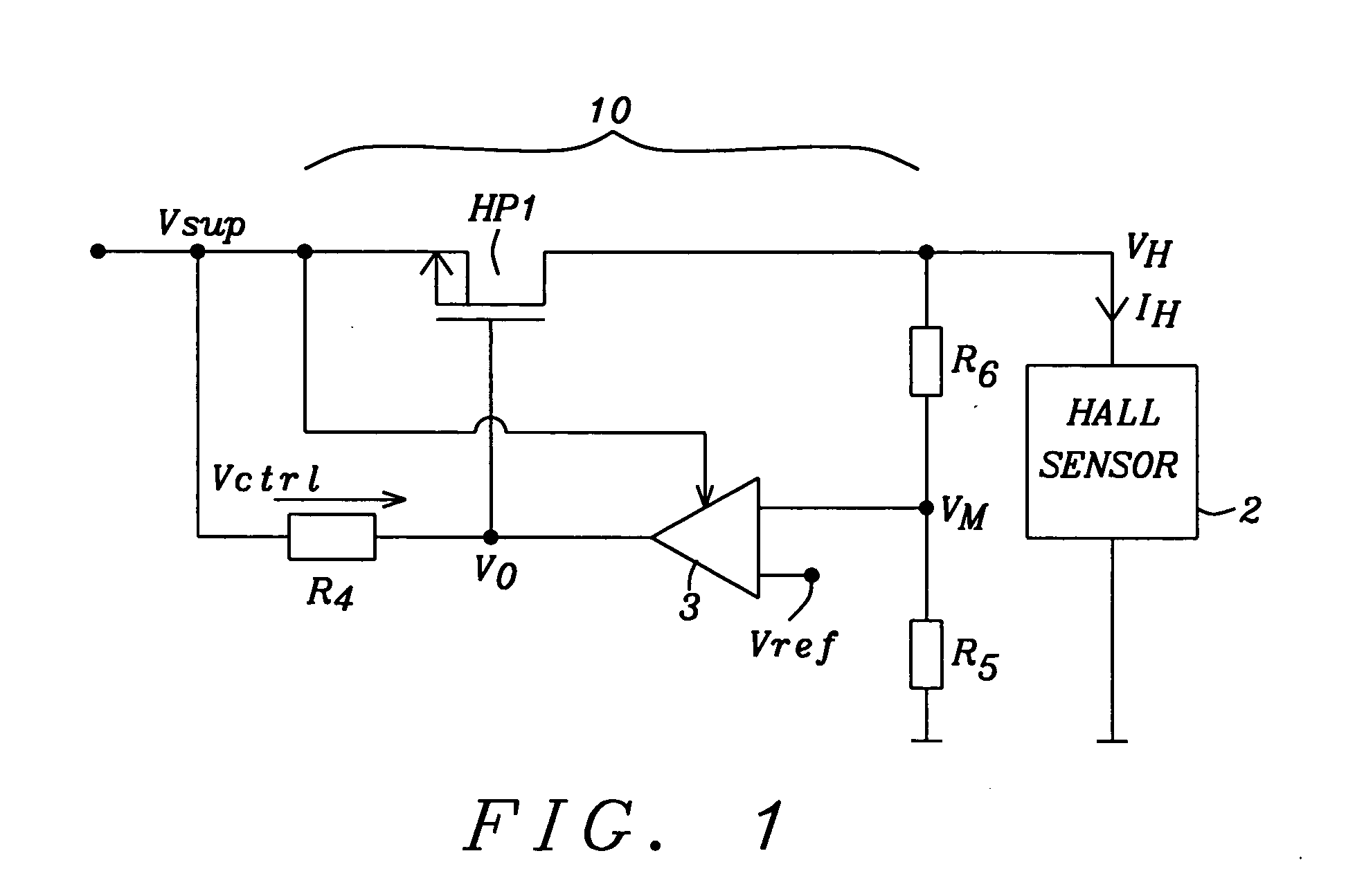
[0026]The preferred embodiments disclose methods and circuits for regulated analog switches to ensure that a supply voltage of a load as e.g. an integrated semiconductor circuit is constant and never exceeds a maximum allowable voltage even in case of a maximum load current. In case a battery voltage is equal or lower than this maximum allowable voltage, the supply voltage of the load is provided with a minimum loss.

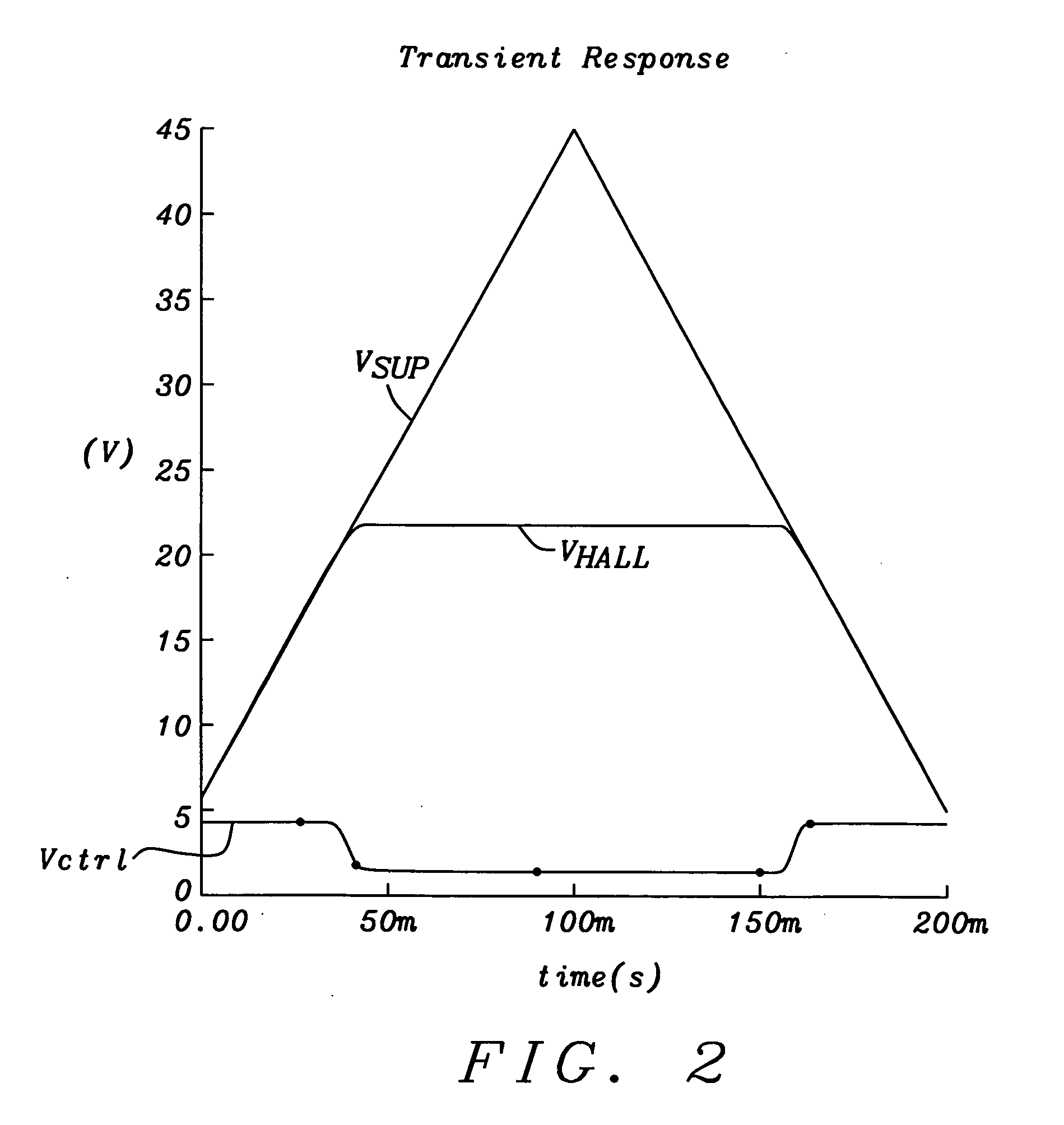
[0027]FIG. 1 shows a schematic illustration of a preferred embodiment of the present invention. It has to be understood that FIG. 1 shows a non-limiting example only of the regulated switch 10 invented. A car battery provides a supply voltage VSUP. This supply voltage VSUP is not constant at all and can have a maximum voltage of 40-60 Volts. In a preferred embodiment a Hall sensor ASIC 2 has a maximum allowable voltage VH of 22 Volts and this voltage has to be kept constant. This means that the gate-source voltage of transistor HP1 of the regulated switch 10 has to be re...


PUM


Abstract

Circuits and methods to achieve a regulated analog switch being capable to provide an output-voltage not exceeding a defined limit are disclosed. In a preferred embodiment a car battery provides a supply voltage up to 40 Volts, wherein a load must not have an output voltage higher than 22 Volts. The drain-source ON-resistance of the switch, realized by a high-voltage MOSFET, is kept to a minimum. The voltage regulation of the preferred embodiment is performed by a single stage operational amplifier and a two-stage amplifier having Miller compensation.

Description

BACKGROUND OF THE INVENTION[0001](1) Field of the Invention[0002]This invention relates generally to analog switches and relates more particularly to a MOSFET switch used in high-voltage applications up to an order of magnitude of 40 Volts protecting a load of excessive voltage and having a minimal drop voltage when battery voltage is not exceeding a threshold voltage critical to a load.[0003](2) Description of the Prior Art[0004]MOSFET analog switches use the MOSFET channels as a low on resistance switch to pass analog signals when on and a high impedance node when off. Signals flow in both directions across a MOSFET switch. In this application the drain and source of a MOSFET switch places depending on the voltages of each electrode compared to that of the gate. For a simple MOSFET without an integrated diode, the source is the most negative side compared to the gate of an N-MOS or the most positive side compared to the gate of a P-MOS. All of these switches are limited on what si...

Claims


Application Information

Patent Timeline
IPC IPC(8): G05F1/00
CPCG05F1/575
Inventor JI, CANG
Owner DIALOG SEMICONDUCTOR GMBH
Why Eureka
Try Eureka