Semiconductor memory device

Inactive Publication Date: 2008-04-24
PANASONIC CORP
View PDF1 Cites 14 Cited by
  • Summary
  • Abstract
  • Description
  • Claims
  • Application Information

AI Technical Summary

Benefits of technology

[0007] In the present invention, the memory cell width is determined according to the transistor pitch in the peripheral control circuit. This permits the transistors of the peripheral control circuit to be arranged without making wasted space, thereby suppressing upsizing of the semiconductor memory device.
[0011] In the above semiconductor memory device, not only the transistors of the peripheral control circuits can be arranged without making wasted space but also the memory capacity can be increased or decreased in columns or rows, thereby facilitating layout change of the memory cell array.
[0013] In the above semiconductor memory device, when the peripheral control circuits are arranged correspondingly to the memory cells arranged in an array, the control lines can be wired straight from the memory cell array to the peripheral control circuits. As a result, the length of the control lines can be shortened to a minimum, thereby suppressing unnecessary addition of a parasitic capacitance and / or a resistance to contemplate high-speed writing or reading operation.
[0015] In the above semiconductor memory device, when the peripheral control circuits are arranged correspondingly to the memory cells arranged in an array, the bit lines and the word lines can be wired straight from the memory cell array to the peripheral control circuits. As a result, the lengths of the bit lines and the word lines can be shortened to minimums, thereby suppressing unnecessary addition of a parasitic capacitance and / or a resistance to contemplate high-speed writing or reading operation.

Problems solved by technology

This makes wasted space in the peripheral control circuit to increase the area of the peripheral control circuit.

Method used


Image

  • Semiconductor memory device
  • Semiconductor memory device
  • Semiconductor memory device

Examples


embodiment 1

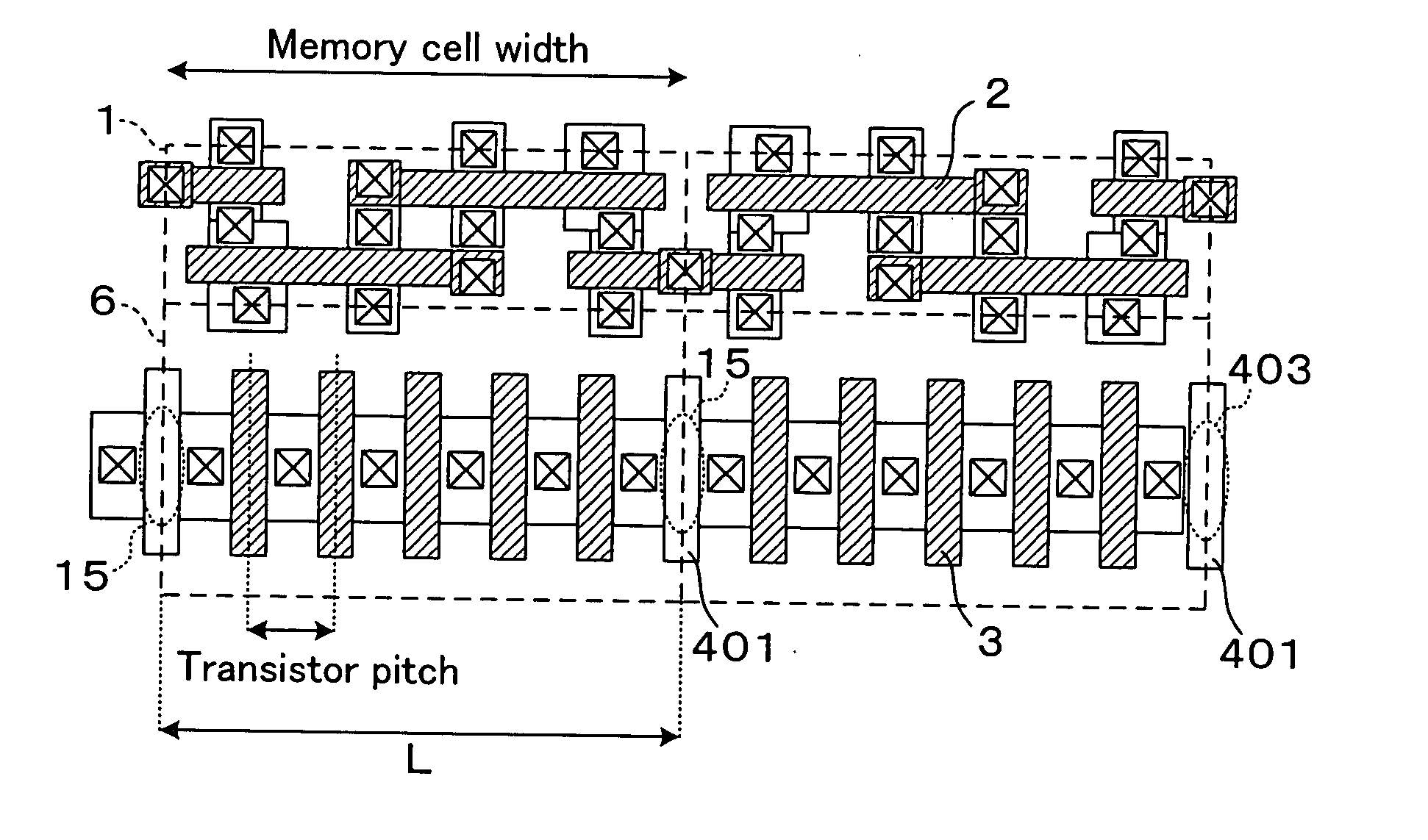
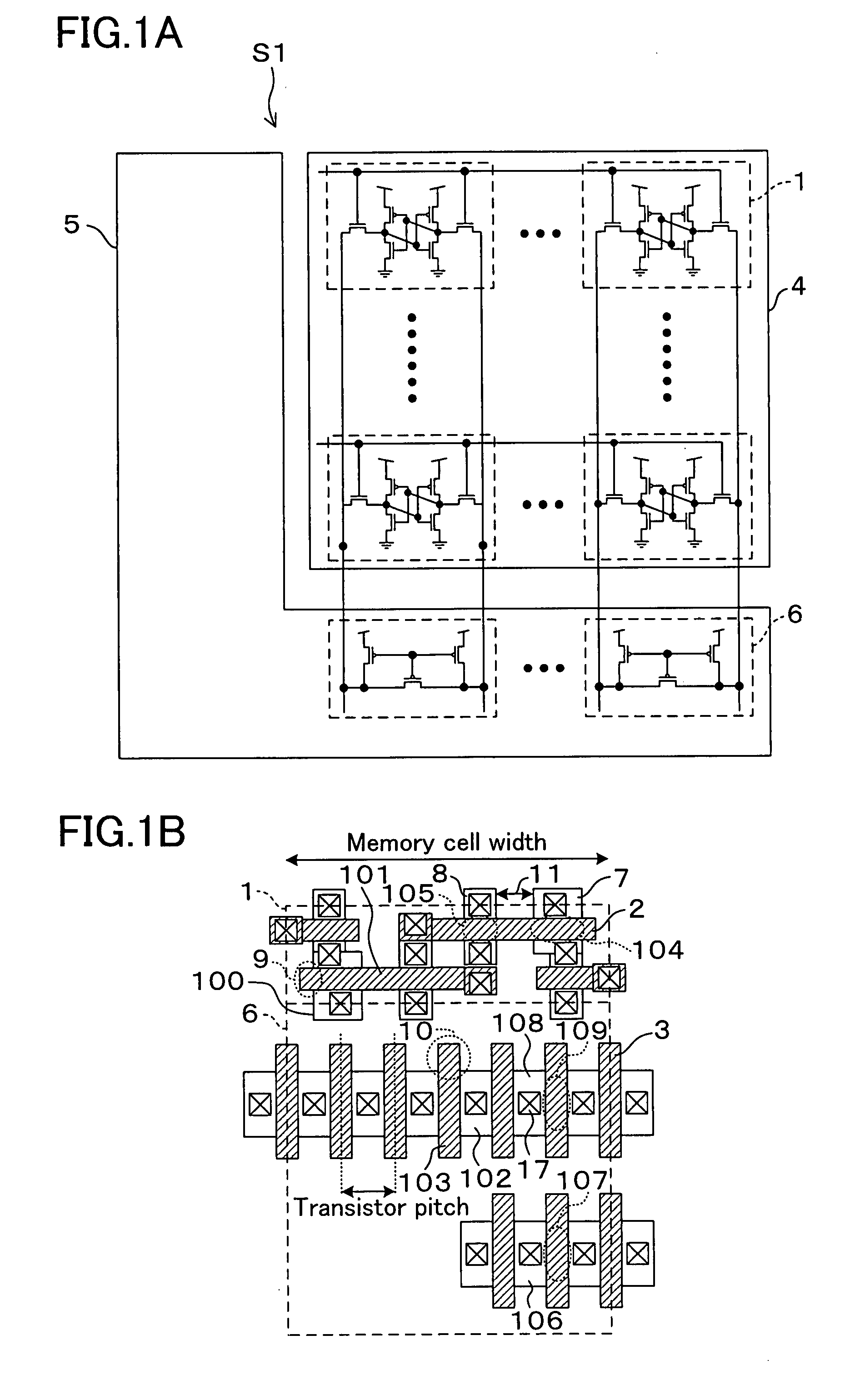
[0027]FIG. 1A is a schematic circuit diagram of a static random access memory (hereinafter referred to it as an SRAM) in Embodiment 1, and FIG. 1B is a diagram showing an arrangement of transistors 2, 2, . . . and transistors 3, 3, . . . composing the SRAM (S1). In FIG. 1A and FIG. 1B, the same reference numerals are assigned to the same elements as those in FIG. 7 for omitting description thereof.

[0028] In FIG. 1A, the SRAM (semiconductor memory device) (S1) is composed of a memory cell array 4 in which memory cells 1, 1, . . . are arranged in rows and columns, a control section 5, a plurality of bit lines, and a plurality of word lines. The drawings also show precharge circuits 6, 6, . . . connected to the bit lines, as one example of peripheral control circuits included in the control section 5. The peripheral control circuits control data reading or writing of the memory cells 1, 1, . . . .

[0029] In FIG. 1B, in each memory cell 1, a plurality of transistors 2, 2, . . . are arr...

embodiment 2

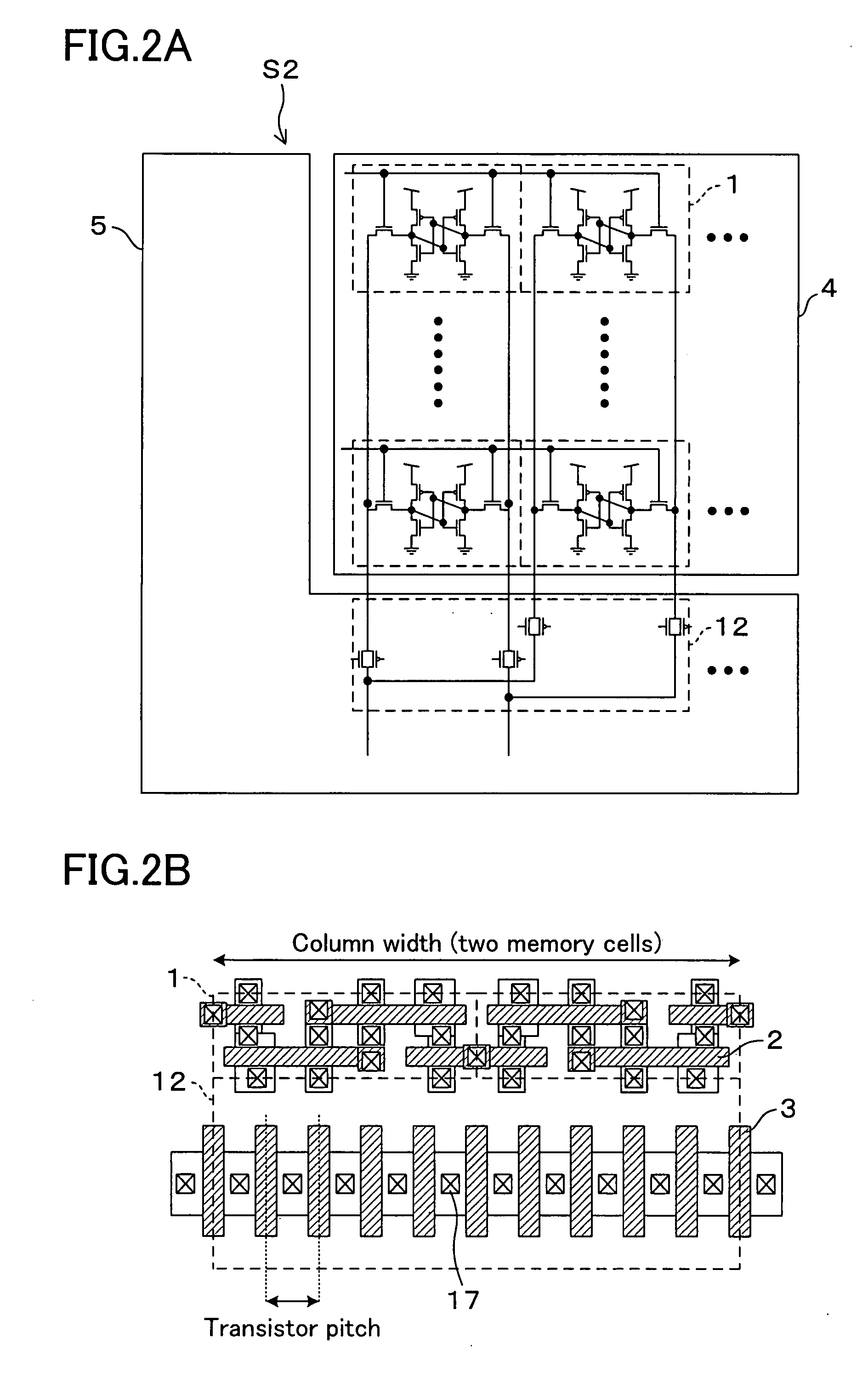
[0039]FIG. 2A is a schematic circuit diagram of a SRAM (S2) in accordance with Embodiment 2, and FIG. 2B is a diagram showing an arrangement of transistors 2, 2, . . . and transistors 3, 3, . . . composing an SRAM (S2). In FIG. 2A and FIG. 2B, the same reference numerals are assigned to the same elements as those in FIG. 1 for omitting description thereof.

[0040] As shown in FIG. 2A, in the present embodiment, column selection circuits 12, 12, . . . (for two columns) are referred to as one example of the peripheral control circuits included in the control section 5.

[0041] Further, as shown in FIG. 2B, a plurality of transistors 3, 3, . . . are provided in each column selection circuit 12, wherein each transistor 3 is arranged so as to extend substantially in parallel with the bit lines at a substantially constant transistor pitch in the column direction of the memory cell array 4.

[0042] The memory cells 1, 1, . . . in the present embodiment are designed so that the width that seve...

embodiment 3

[0044]FIG. 3A is a schematic circuit diagram of a SRAM (S3) in accordance with Embodiment 3, and FIG. 3B is a diagram showing an arrangement of transistors 2, 2, . . . and transistors 3, 3, . . . composing an SRAM (S3). In FIG. 3A and FIG. 3B, the same reference numerals are assigned to the same elements as those in FIG. 1 for omitting description thereof.

[0045] As shown in FIG. 3A, in the present embodiment, word line drive circuits 13, 13 . . . are referred to as one example of the peripheral control circuits included in the control section 5.

[0046] As further shown in FIG. 3B, six transistors are provided in each memory cell 1, wherein two of the six are N-channel transistors 14, 14 while the other four are P-channel transistors. Each of the N-channel transistors and the P-channel transistors includes a gate electrode. Each gate electrode of the N-channel transistors 14, 14 is arranged substantially in parallel with the word lines while each gate electrode of the P-channel tran...


PUM


Abstract

A semiconductor memory device includes a memory cell array and peripheral control circuits. In each of the peripheral control circuits, a plurality of transistors are arranged at a substantially constant transistor pitch in a first direction which is the row direction or the column direction of the memory cell array. In the memory cell array, a memory cell length in the first direction is substantially n times the transistor pitch, wherein n is an integer.

Description

BACKGROUND OF THE INVENTION [0001] 1. Field of the Invention [0002] The present invention relates to semiconductor memory devices, and particularly relates to a semiconductor memory device including a memory cell array and a peripheral control circuit. [0003] 2. Background Art [0004]FIG. 7 shows a layout of a memory cell and a peripheral control circuit in a conventional semiconductor memory device. The transistor pitch in the peripheral control circuit is set constant in order to suppress variation in gate length of the transistors, as disclosed in Japanese Patent Application Laid Open Publication No. 9-289251, for example. [0005] In FIG. 7, transistors 2, 2, . . . of a memory cell 1 are arrange perpendicularly to transistors 3, 3, . . . of the peripheral control circuit, and the cell width of the memory cell 1 is smaller than the width occupied by the transistors 3, 3, . . . arrange at a transistor pitch. When a memory cell array is formed by arranging a plurality of memory cells ...

Claims


Application Information

Patent Timeline
IPC IPC(8): G11C5/06G11C7/00G11C8/00
CPCG11C5/063H01L27/1104H01L27/11G11C11/412H10B10/00H10B10/12
Inventor TSUJIMURA, KAZUKIOKUYAMA, HIROAKI
Owner PANASONIC CORP
Why Eureka
Try Eureka