Inspection apparatus and an inspection method

a technology of inspection apparatus and inspection method, which is applied in the direction of image enhancement, instruments, nuclear engineering, etc., can solve the problems of difficult to distinguish between microscopic defects and noise, diversified material and configurations of circuit pattern formation,

Inactive Publication Date: 2008-05-01
HITACHI HIGH-TECH CORP
View PDF19 Cites 23 Cited by
  • Summary
  • Abstract
  • Description
  • Claims
  • Application Information

AI Technical Summary

Benefits of technology

[0010] According to the present invention, it becomes possible to perform the semiconductor wafer inspection under a suitable condition even if the intensity of secondary electrons or reflected electrons changes in time.

Problems solved by technology

Materials and configurations of which a circuit pattern is formed have been diversified and complicated.
When the S / N ratio is lowered, it becomes difficult to distinguish between the microscopic defects and noises.

Method used


Image

  • Inspection apparatus and an inspection method
  • Inspection apparatus and an inspection method
  • Inspection apparatus and an inspection method

Examples


1st embodiment

(Inspection Target)

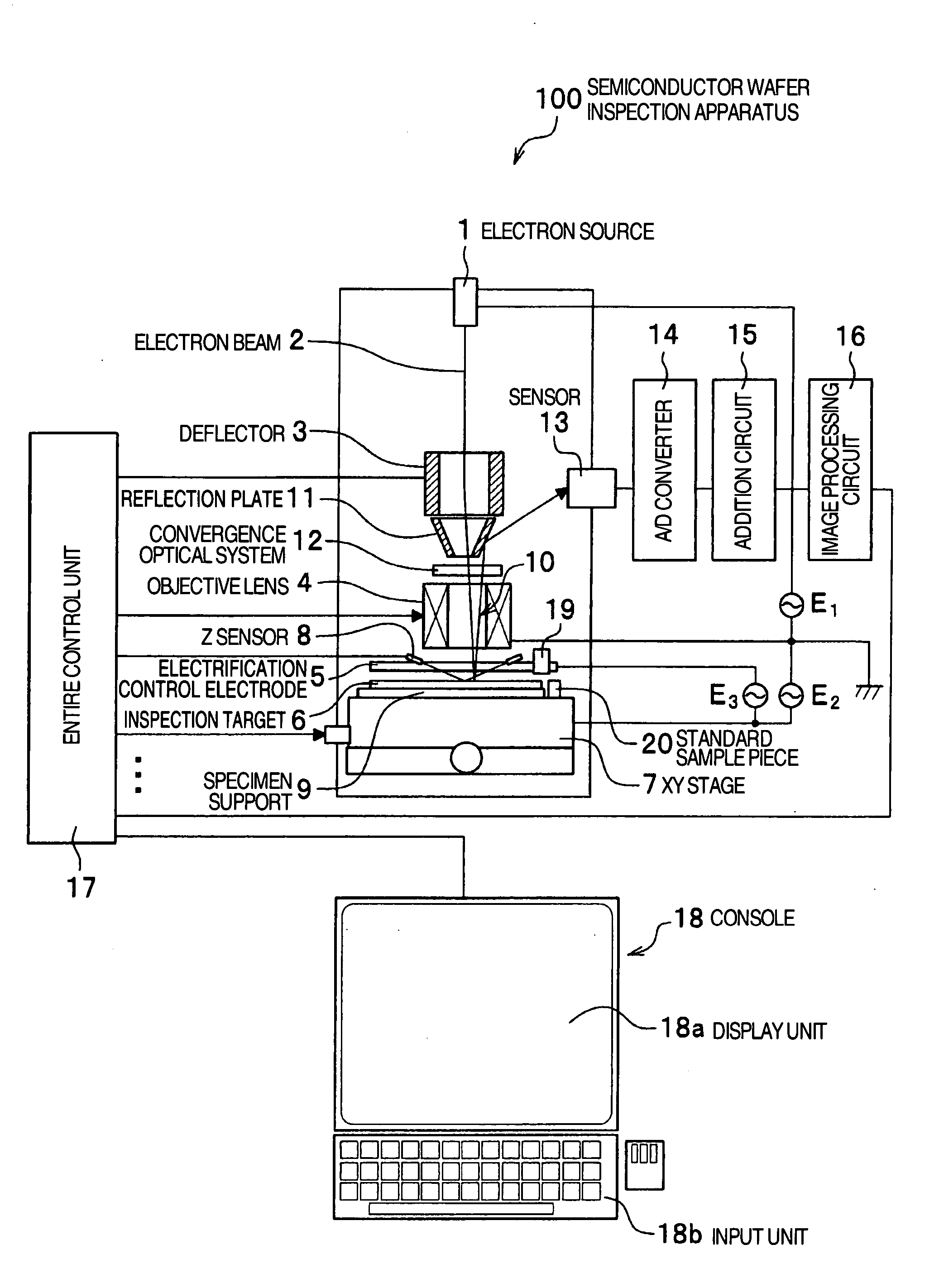
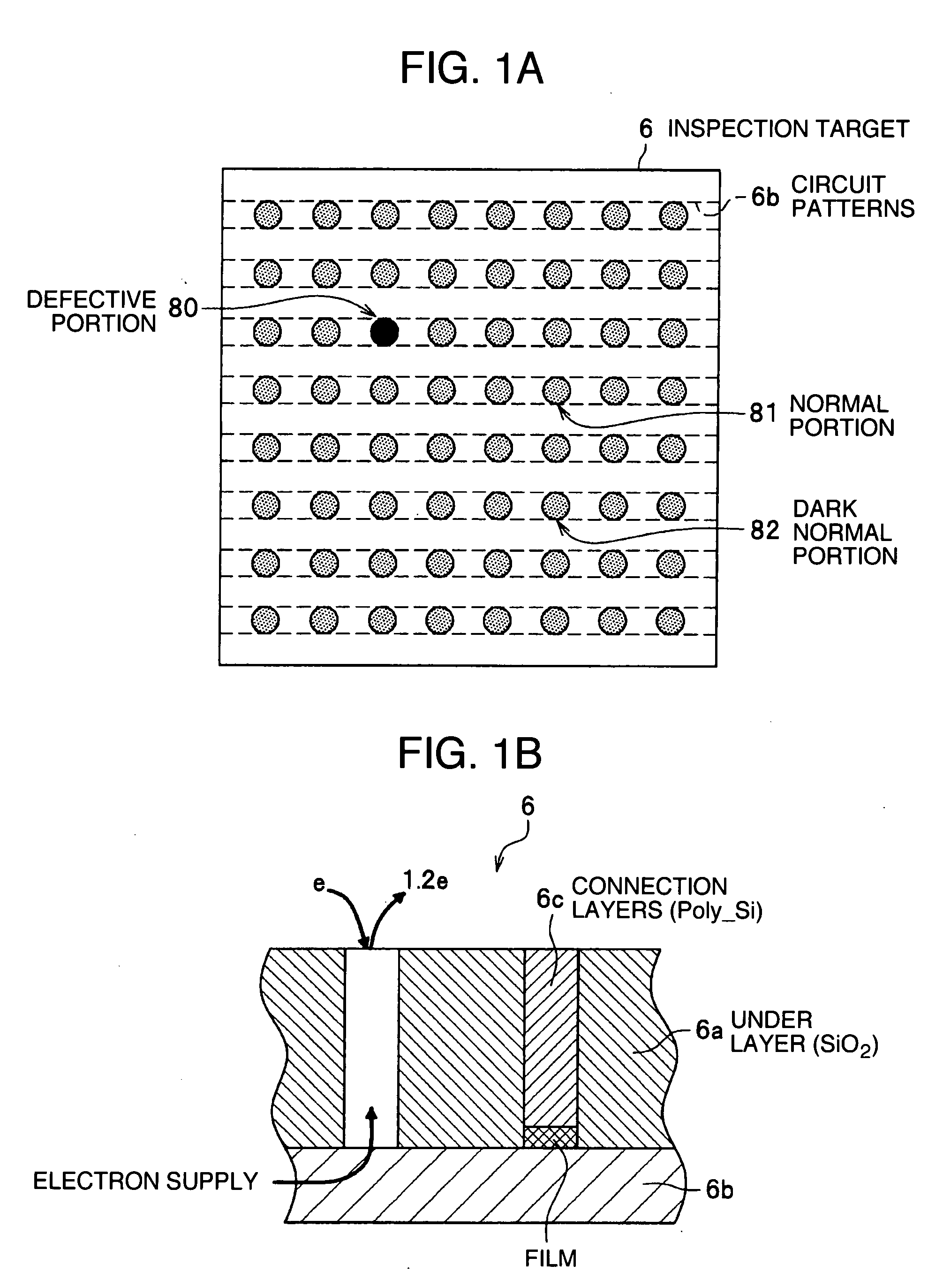
[0026] First, referring to FIG. 1A and FIG. 1B, the explanation will be given below concerning an inspection target of a semiconductor wafer inspection apparatus which is an embodiment of the present invention. FIG. 1A is a plan view of a semiconductor wafer, i.e., the inspection target, and FIG. 1B is a cross-sectional view thereof. Incidentally, the semiconductor wafer, which is of about-300-mm-diameter and about-1-mm-thick disc shape, is formed by arranging side by side a few hundreds of about-1-cm-square-size dies. These dies are units each of which is equipped with one and the same circuit pattern, and which finally become commercial products with the same model number by being cut off. Each die includes in its inside a pattern having a constant repetition such as a memory portion, and a circuit with scarce repetition property. Pattern comparison inspection is generally used for the inspection of a circuit pattern like this. In the pattern comparison inspec...

2nd embodiment

[0054] A semiconductor wafer inspection apparatus which is a second embodiment of the present invention includes basically the same configuration as that of the semiconductor wafer inspection apparatus 100 illustrated in the first embodiment. The semiconductor wafer inspection apparatus 150 illustrated in FIG. 13, however, differs from the semiconductor wafer inspection apparatus 100 illustrated in the first embodiment in a point that it includes an image storage unit 70 and a time-sequence defect memory 71. Here, the image storage unit 70 is provided between the A / D converter 14 and the image processing circuit 16, and the time-sequence defect memory 71 stores time-sequence defect information in proximity to a point judged to be a defect. Also, a block diagram illustrated in FIG. 14 also differs from FIG. 4 in the point that it includes the image storage unit 70, and the division circuit 16a, an addition circuit 16c, and a subtractor 16d, which are provided inside the image process...


PUM


Abstract

An inspection apparatus includes an irradiation optical system for irradiating an inspection target with an electron beam, a scanning unit for scanning an irradiation position in the X direction and the Y direction, an electrification control electrode for controlling secondary electrons or reflected electrons generated on the inspection target by the irradiation with the electron beam, a sensor for detecting the secondary electrons or the reflected electrons, an A/D converter for sequentially converting the signals into digital image signals from an irradiation start point-in-time of the electron beam, an addition circuit for creating a detection image by adding the digital image signals from a first set point-in-time to a second set point-in-time on each pixel basis, and an image processing circuit for judging a defect by comparing the detection image with a reference image of a circuit pattern formed on the inspection target.

Description

BACKGROUND OF THE INVENTION [0001] 1. Field of the Invention [0002] The present invention relates to a semiconductor wafer inspection apparatus and its inspection method for inspecting defects of an inspection target having a circuit pattern, using an electron beam. [0003] 2. Description of the Related Art [0004] An embodiment of conventional electron-beam type pattern inspection apparatuses is disclosed in JP-A-5-258703 (U.S. Pat. No. 5,502,306). This electron-beam type pattern inspection apparatus irradiates a semiconductor wafer of the inspection target with an electron beam, then detecting secondary electrons generated on the surface of the semiconductor wafer. Also, this electron-beam type pattern inspection apparatus scans the electron beam, thereby making it possible to acquire a secondary-electron image of the circuit pattern on the semiconductor wafer. Moreover, the electron-beam type pattern inspection apparatus compares the detected inspection image with a reference image...

Claims


Application Information

Patent Timeline
Patent Type & Authority Applications(United States)
IPC IPC(8): G21K5/04
CPCG06T7/001G06T2200/24H01J2237/2817G06T2207/30148G06T2207/10061
Inventor HIROI, TAKASHIMIYAI, HIROSHIITO, HIROKAZUNAKANO, MICHIO
Owner HITACHI HIGH-TECH CORP
Why Eureka
Try Eureka