Semiconductor structure with increased breakdown voltage and method for producing the semiconductor structure

Inactive Publication Date: 2006-02-21
INFINEON TECH AG
View PDF4 Cites 16 Cited by
  • Summary
  • Abstract
  • Description
  • Claims
  • Application Information

AI Technical Summary

Benefits of technology

[0021]It is another advantage of the present invention that two transistors can be integrated simultaneously, one of which can be optimized with regard to HF performance and the other one can be optimized separately with regard to the breakdown voltage. In the conventional method, either the HF performance of the HF transistor suffers, or the breakdown voltage of the HV transistor is too low.
[0022]It is another advantage off the present invention that the dimensions of the inventive semiconductor structure are smaller in comparison to the dimensions of the structure according to the prior art discussed in FIG. 8, since a thickness of the second semiconductor layer, which can, for example, be a collector epitaxial layer, is not chosen based on the breakdown voltages of the HV transistor but based on the HF performance of the HF transistor, so that the thickness of the second semiconductor layer is smaller, which leads to a further reduction of production costs.
[0023]It is another advantage of the inventive semiconductor structure that it enables HF transistors with optimized HF properties and HV transistors with a sufficient breakdown voltage strength integrated in one circuit.
[0024]Another advantage of the present invention is a reduction of production costs of the inventive semiconductor structure, since less production steps as well as thinner layers (collector epilayer) are sufficient for achieving an optimum HF performance of the HF transistors as well as a sufficient breakdown voltage of the HV tran

Problems solved by technology

Since the low doping for the HF transistor does not allow sufficiently high collector currents and thus the HF performance suffers as well, since a maximum cutoff frequency ft (transit frequency) depends in a linear way on a maximum collector current Ic, where the so-called Kirk effect occurs, often a so-called SIC (SIC=selectively implanted collector) is implanted in a conventional HF transistor.
A disadvantage is, that the HF performance of the transistor is affected thereby, since, on the one hand, the doping and thus a conductivity of the SIC is significantly lower in comparison to the subcollector.
On the other hand, the SIC implantation cannot nearly achieve a dopant profile as high as by an epitaxy, so that a collector resistance is higher than with a minimal possible epithickness.
All in all, the HF transistor does not achieve the best possible performance, which would be possible in this technology generation, since, for example, the already mentioned increased collector resistance as well as the higher minority charge carrier storage lower the cutoff frequency of the HF transistor.
It is another disadvantage of the approach illustrated in FIG. 8 that the HF properties of the HF transistor starting from the HV transistor, whose collector epitaxy is optimally designed for increasing the breakdown voltage, are to be improved by an introduction of one or several SICs, respectively.
Thi

Method used


Image

  • Semiconductor structure with increased breakdown voltage and method for producing the semiconductor structure
  • Semiconductor structure with increased breakdown voltage and method for producing the semiconductor structure
  • Semiconductor structure with increased breakdown voltage and method for producing the semiconductor structure

Examples


Embodiment Construction

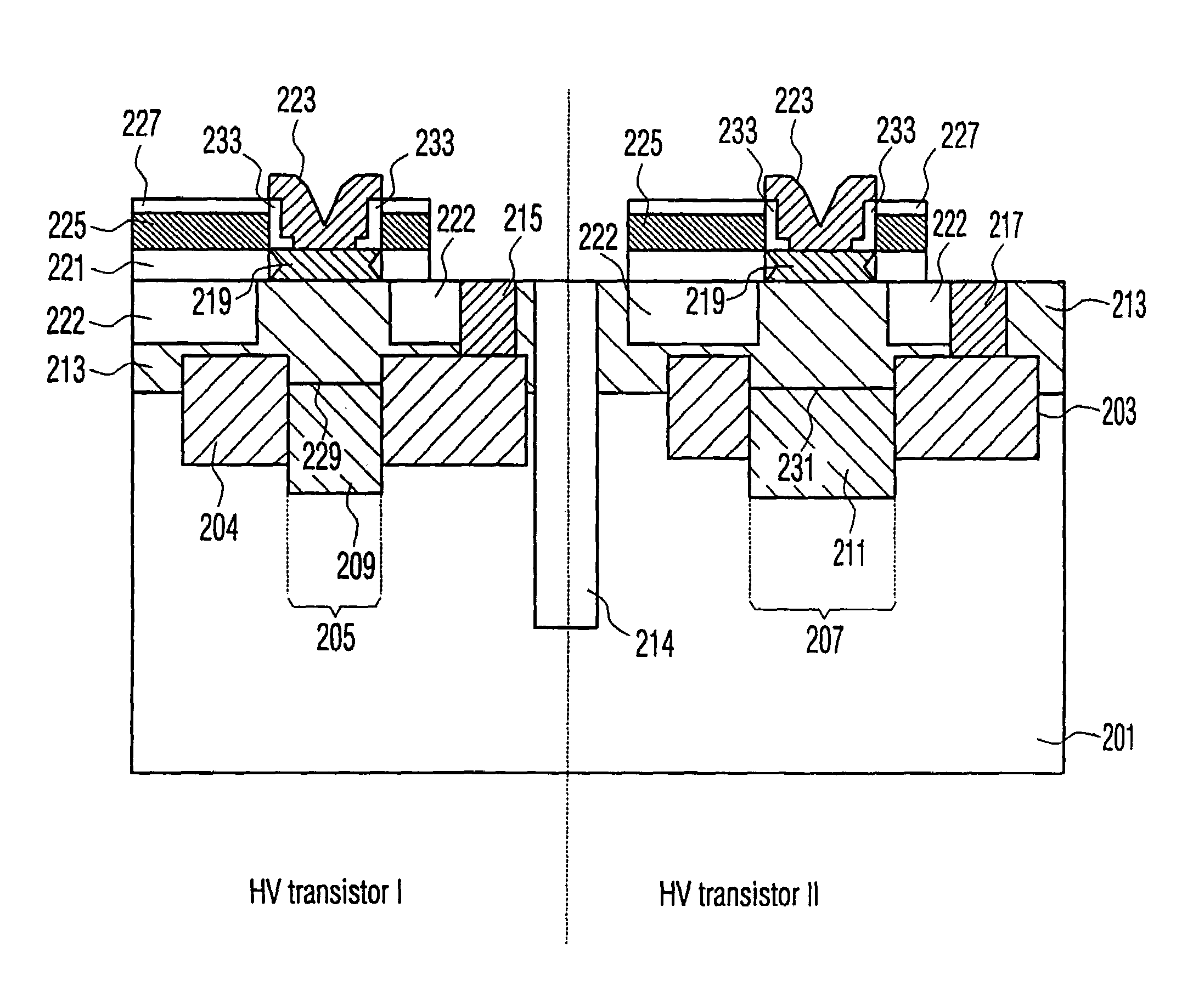
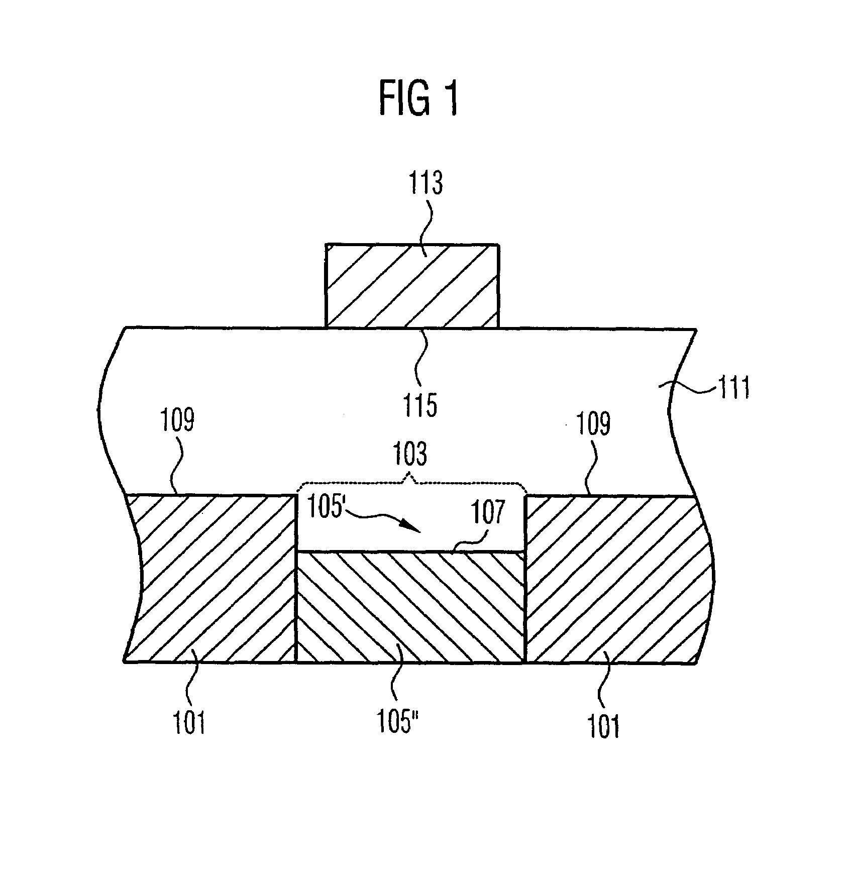
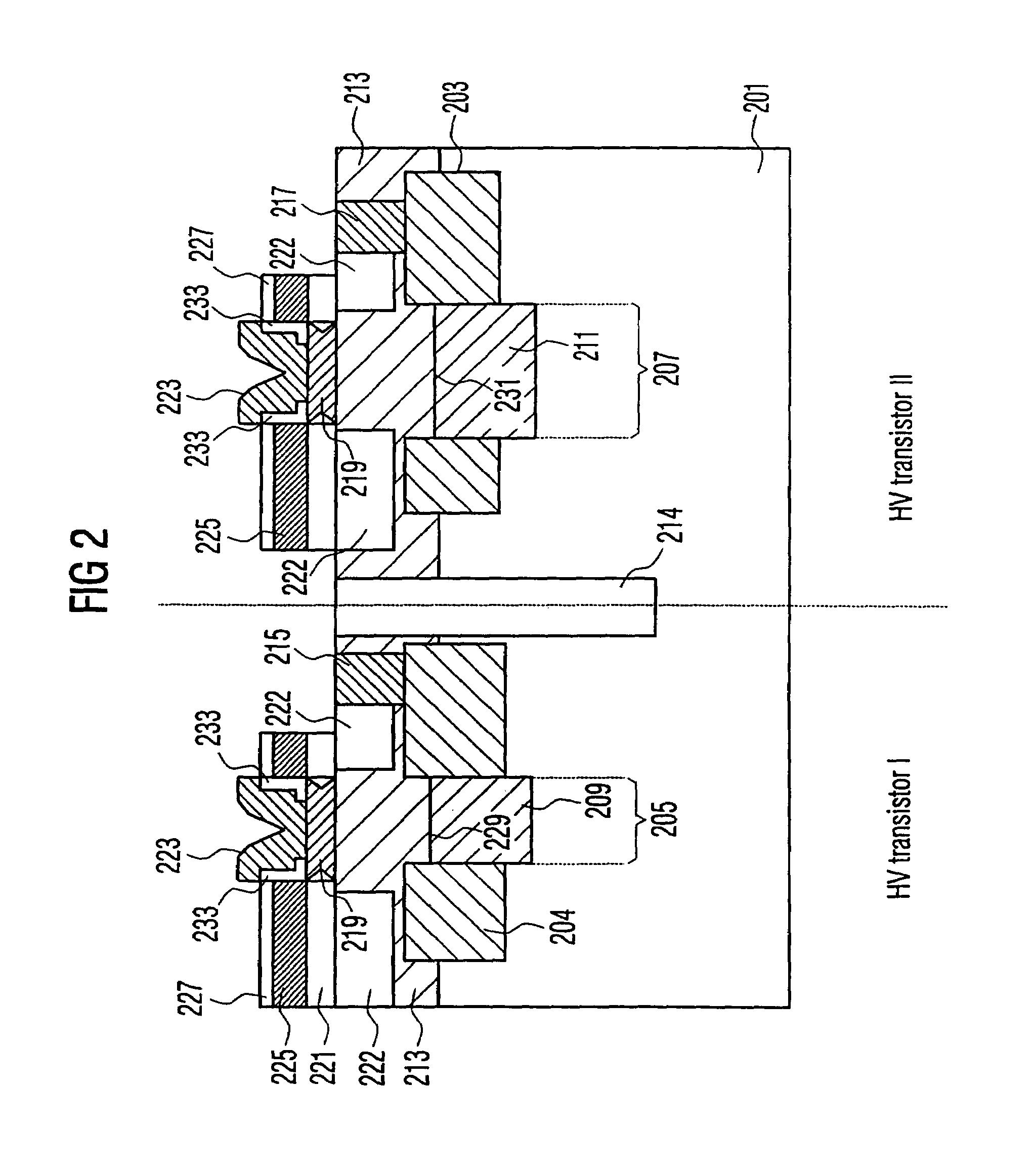
[0036]FIG. 1 shows a first embodiment of a semiconductor structure according to the present invention. The semiconductor structure comprises a heavily doped buried first semiconductor layer 101 of a first doping type, wherein a recess 103 is formed. On a first surface 109 of the buried first semiconductor layer 101, as well as on the top surface 107 of the further semiconductor area 105″, a second semiconductor layer 111 is formed, which is a weakly doped layer of the first doping type, which can, for example, be an epi layer. The second weakly doped semiconductor layer extends into a portion 105′ of the recess 103. Further, another semiconductor area 105″ of the first doping type is disposed in the recess 103, whose doping density lies preferably between the epi layer 111 and the buried layer 101, and which preferably lies deeper than the buried first semiconductor layer 101. The further semiconductor area 105″ further comprises a top surface 107.

[0037]A semiconductor area 113 with...


PUM


Abstract

A semiconductor structure comprises a buried first semiconductor layer of a first doping type, a second semiconductor layer of the first doping type on the buried semiconductor layer, which is less doped than the buried first semiconductor layer, a semiconductor area of a second doping type on the second semiconductor layer, so that a pn junction is formed between the semiconductor area and the second semiconductor layer, and a recess present below the semiconductor area in the buried first semiconductor layer, which comprises a semiconductor material of the first doping type, which can be less doped than the buried first semiconductor layer and has a larger distance to the semiconductor area of the second doping type on the second semiconductor layer, such that the breakdown voltage across the pn junction is higher than if the recess were not provided. Thereby, it is achieved that both a semiconductor structure with a desired breakdown voltage as well as a further semiconductor structure without this recess can be generated in the buried first semiconductor layer with optimized HF properties.

Description

BACKGROUND OF THE INVENTION[0001]1. Field of the Invention[0002]The present invention relates to a semiconductor structure with increased breakdown voltage across a pn junction, which the semiconductor structure comprises.[0003]2. Description of the Prior Art[0004]One of the main demands on semiconductor structures in modern microelectronic circuits is that the semiconductor structures ideally have a desired breakdown strength matched with a good frequency characteristic, such as a high cutoff frequency, for a respective application.[0005]Particularly in modern BiCMOS technologies, where a collector of a bipolar transistor is laterally connected via a heavily doped subcollector (buried layer), which is buried by a collector epitaxy, often mutually exclusive demands are made on a bipolar process module. On the one hand, an integration of a bipolar transistor, which is as fast as possible, is required for low operating voltages, on the other hand, usually, bipolar transistors are requ...

Claims


Application Information

Patent Timeline
IPC IPC(8): H01L21/8238H01L21/8222H01L27/082H01L29/08H01L29/732
CPCH01L21/8222H01L29/732H01L29/0821H01L27/0825
Inventor TILKE, ARMINKLEIN, WOLFGANG
Owner INFINEON TECH AG
Why Eureka
Try Eureka