Multilayer wiring substrate mounted with electronic component and method for manufacturing the same

a technology of multi-layer wiring and electronic components, which is applied in the manufacture of printed circuits, printed circuit aspects, basic electric elements, etc., can solve the problems of reducing the thickness of multi-layer wiring substrates. achieve the effect of reducing thicknesawiring

Inactive Publication Date: 2008-05-01
SHINKO ELECTRIC IND CO LTD
View PDF2 Cites 40 Cited by
  • Summary
  • Abstract
  • Description
  • Claims
  • Application Information

AI Technical Summary

Benefits of technology

[0010] Exemplary embodiments of the present invention provide a multilayer wiring substrate which enables appropriate incorporation of an electronic component in a wiring substrate main body even in the case of the multilayer wiring substrate formed by electrically connecting the electronic component to the wiring substrate main body by wire bonding and can have the reduced thicknesawiring.

Problems solved by technology

However, in relation to the related-art wiring substrate with built-in electronic components, a configuration for preferably incorporating electronic components to be connected to a wiring pattern by means of wire bonding has never been described.
Therefore, a sealing section, or the like, requires a thickness for housing the loops, which in turn hinders miniaturization of a module substrate during formation thereof.
Moreover, the surface of the formed resin sealing material layer has a low degree of smoothness, and mounting electronic components, such as surface mount devices, on the sealing material layer is impracticable.
However, in connection with a multilayer wiring substrate in which electronic components are mounted on a wiring substrate and in which the electronic components and conductor sections for connection purpose (hereinafter called “connection conductor sections”) of the substrate are electrically connected by means of wire bonding, the multilayer wiring substrate which achieves a sufficient reduction in thickness has never been disclosed.

Method used


Image

  • Multilayer wiring substrate mounted with electronic component and method for manufacturing the same
  • Multilayer wiring substrate mounted with electronic component and method for manufacturing the same
  • Multilayer wiring substrate mounted with electronic component and method for manufacturing the same

Examples


first embodiment

[0079]FIGS. 1 through 12 show a method for manufacturing a multilayer wiring substrate mounted with electronic components according to the present invention.

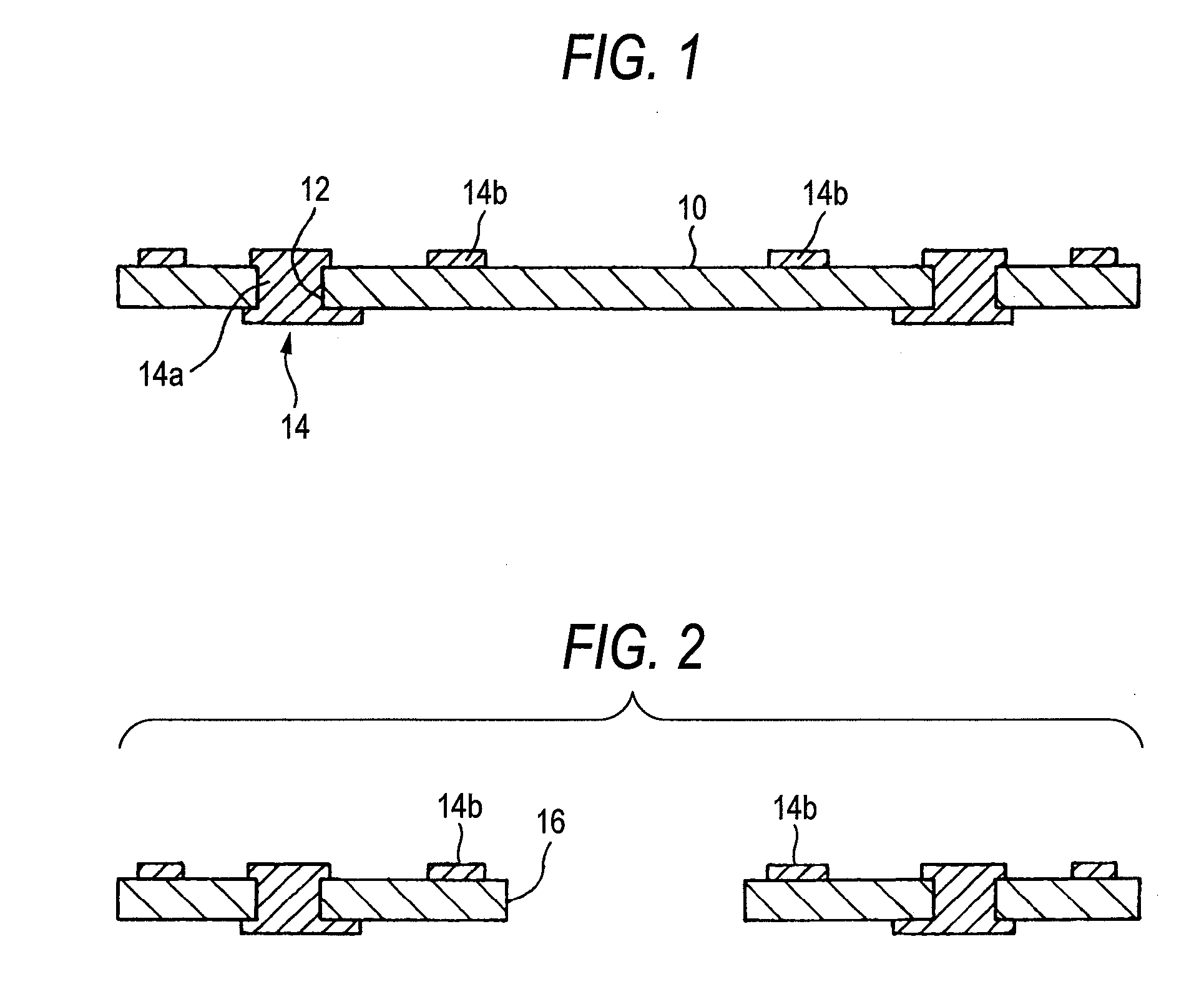
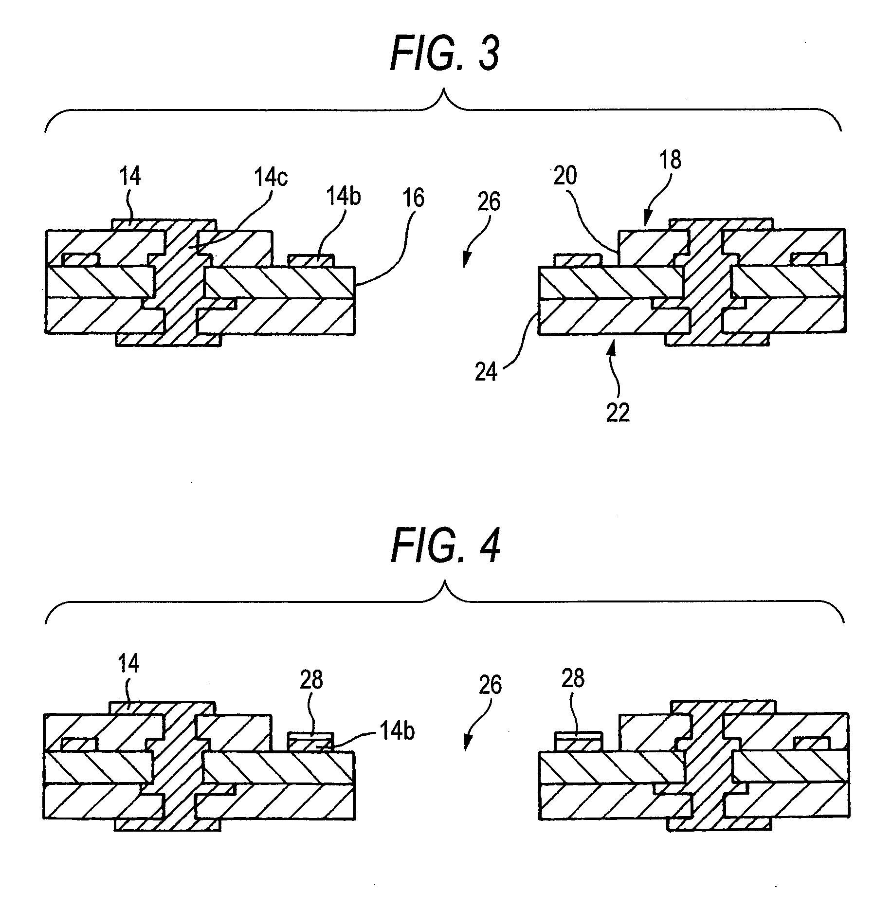
[0080]FIG. 1 shows a core material in which a wiring pattern is formed. A plate-like core material 10, which is formed from a glass epoxy material, or the like, and which is usually used as a material of a wiring substrate, is prepared, and through holes 12 are formed in the core material 10 by means of a well-known appropriate method. The core material 10 including the through holes 12 is plated with copper, or the like. A copper plating layer is patterned by means of a subtractive process, thereby forming a required wiring pattern 14 including conductor vias 14a which penetrates through the through holes 12. A plurality of connection pads 14b, which are to serve as connection conductor sections to be connected to electronic components to be mounted by means of wire bonding in a subsequent process, are also formed simultaneousl...

second embodiment

[0099]FIG. 13 shows a state where the copper foil 30 is exfoliated and removed and then the insulating resin layer is formed on both surfaces of the core material. The electronic components 34 are mounted on the substrate (FIG. 6), and the openings 26 and the 20 are filled with the sealing resin 40, to thus seal the electronic components 34 and the bonding wires 38 in an insulated manner (FIG. 7). Subsequently, in the second embodiment, the copper foil 30 acting as a supporting layer in FIG. 13 when the electronic components 34 are mounted is dissolved and removed by use of an etchant which dissolves; for example, copper. However, a range over which the copper foil 30 is dissolved is partially limited, and only a portion of the copper foil 30 is left in only the areas corresponding to the lower surfaces where the electronic components 34 are mounted. Specifically, when the copper foil 30 is dissolved and removed from the back surface by use of an etchant, a treatment is temporarily ...

third embodiment

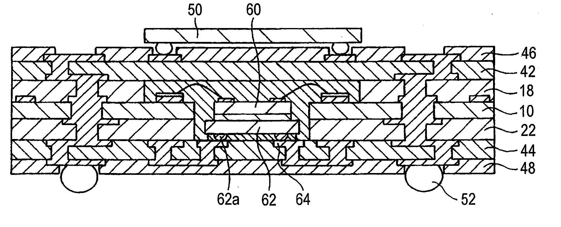
[0121]FIG. 24 shows a state where a surface mount component is mounted and where external connection terminals are formed. As in the case of the previous embodiments, in a multilayer wiring substrate mounted with an electronic component of the third embodiment sliced as one semiconductor device unit, a surface mount component 50 is mounted by way of the connection pads 46a and by means of a surface mount technique (SMT), or the solder bumps 52 are formed on the connection pads 48a used for connection with external connection terminals.

[0122] In addition to yielding the same working-effect as that yielded in the first and second embodiments, the multilayer wiring substrate mounted with an electronic component of the third embodiment of the present invention enables mounting of, on a multilayer wiring substrate, an electronic component of wire bonding type and an electronic component of stack type, such as a surface mount electronic component, which differ from each other in terms of ...


PUM


Abstract

A multilayer wiring substrate mounted with an electronic component includes an electronic component, a core material layer having a first opening for accommodating the electronic component, a resin layer which is formed on one surface of the core material layer and which has a second opening greater than the first opening, a supporting layer which is formed on the other surface of the core material layer and which supports the electronic component, a plurality of connection conductor sections which are provided around the first opening and within the second opening on the one surface of the core material layer, bonding wires for electrically connecting the electronic component to the connection conductor sections, and a sealing resin filled into the first and second openings in order to seal the electronic component and the bonding wires.

Description

[0001] This application claims priority to Japanese Patent Application No. 2006-286300, filed Oct. 20, 2006, in the Japanese Patent Office. The priority application is incorporated by reference in its entirety. TECHNICAL FIELD [0002] The present disclosure relates to a multilayer wiring substrate mounted with an electronic component and a method for manufacturing the substrate. Particularly, the present disclosure relates to a multilayer wiring substrate mounted with an electronic component in which a plurality of electrode terminals of the electronic component and a plurality of connection conductor sections of a substrate main body are connected together by means of wire bonding, as well as to a method for manufacturing the same. RELATED ART [0003] Wiring substrates, such as those described in connection with Patent Documents 1 through 3 provided below, have hitherto been known as a wiring substrate with built-in electronic components such as semiconductor elements. However, in re...

Claims


Application Information

Patent Timeline
Patent Type & Authority Applications(United States)
IPC IPC(8): H01L23/49H01L21/52
CPCH01L23/13H01L23/49822H01L2924/15311H01L2924/07802H01L2224/45144H01L24/48H05K2203/049H05K2201/09845H05K3/4602H05K1/186H01L2924/19041H01L2924/1517H01L2924/15153H01L2924/01079H01L2924/01078H01L2224/73265H01L2224/73204H01L2224/48227H01L2224/48091H01L2224/32225H01L2224/32145H01L2224/16225H01L23/5389H01L2924/00014H01L2924/00H01L2924/00012H01L24/45H01L24/73H01L2224/32245H01L2224/45124H01L2224/45147H01L2224/73253H01L2924/00011H01L2924/12042H01L2924/14H01L2924/181H01L2224/0401H05K3/46
Inventor MACHIDA, YOSHIHIRO
Owner SHINKO ELECTRIC IND CO LTD
Why Eureka
Try Eureka