Delay locked loop of semiconductor device and method for driving the same

a technology of delay and lock loop, which is applied in the direction of pulse manipulation, pulse technique, instruments, etc., can solve the problems of clock skew, dll may operate abnormally, and error corresponding to an offset from 50% reduces the timing margin of high-performance memory systems

Active Publication Date: 2008-05-01
SK HYNIX INC
View PDF15 Cites 11 Cited by
  • Summary
  • Abstract
  • Description
  • Claims
  • Application Information

AI Technical Summary

Benefits of technology

[0022]In accordance with still another aspect of the present invention, there is provided a method for driving a delay locked loop (DLL), including: delaying a first clock signal in synchronization with a first edge of an external clock signal to generate a first delayed clock signal; delaying a second clock signal in synchronization with a second edge of an external clock signal to generate a second delayed clock signal; correcting a duty cycle by mixing phases of the first and second delayed clock signals to output a DLL clock signal with a corrected duty cycle; and controlling the correcting of the duty cycle by generating a DCC off signal based on the first and second delayed clock signals.

Problems solved by technology

If the duty cycle of the DLL clock signal (CLK_DLL) is not maintained at 50%, an error corresponding to an offset from 50% reduces a timing margin of a high-performance memory system.
Meanwhile, as the semiconductor device operates faster, the incoming external clock signal (CLK_EXT) becomes distorted, leading to clock skew.
Due to the clock skew in the duty cycle, the DLL may operate abnormally.
Further, the duty cycle problem may occur in the DLL in itself.
Consequently, a desired DLL clock signal (CLK_DLL) may not be outputted, which degrades performance of the semiconductor device.
Consequently, this leads to a defective semiconductor device.

Method used


Image

  • Delay locked loop of semiconductor device and method for driving the same
  • Delay locked loop of semiconductor device and method for driving the same
  • Delay locked loop of semiconductor device and method for driving the same

Examples


Embodiment Construction

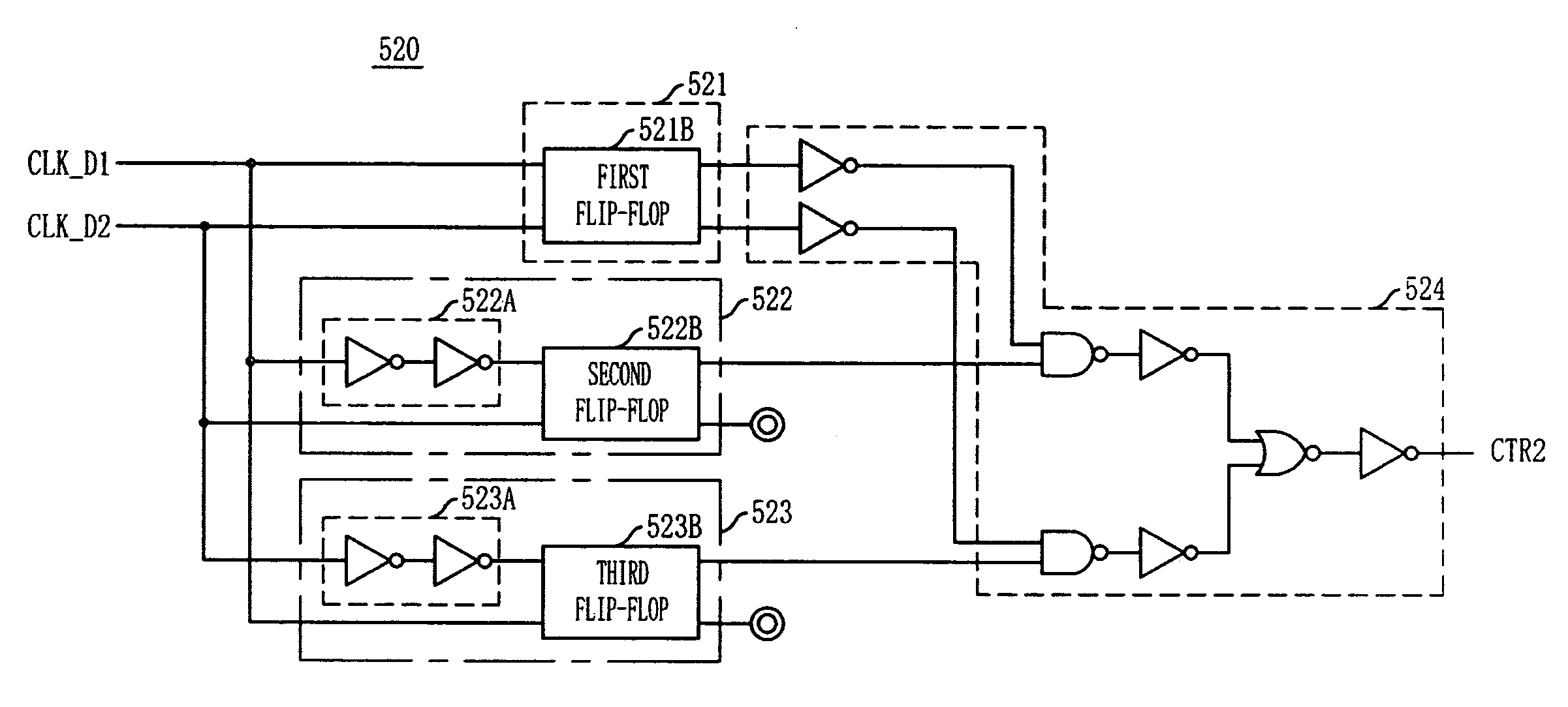
[0030]Hereinafter, a delay locked loop (DLL) having a duty cycle corrector (DCC) in accordance with exemplary embodiments of the present invention will be described in detail with reference to the accompanying drawings.

[0031]FIG. 3 is a block diagram of a DLL in accordance with an embodiment of the present invention.

[0032]Referring to FIG. 3, the DLL includes first and second delay lines 100 and 200, a DCC phase mixer 300, a dummy DCC phase mixer 400, and a DCC controller500.

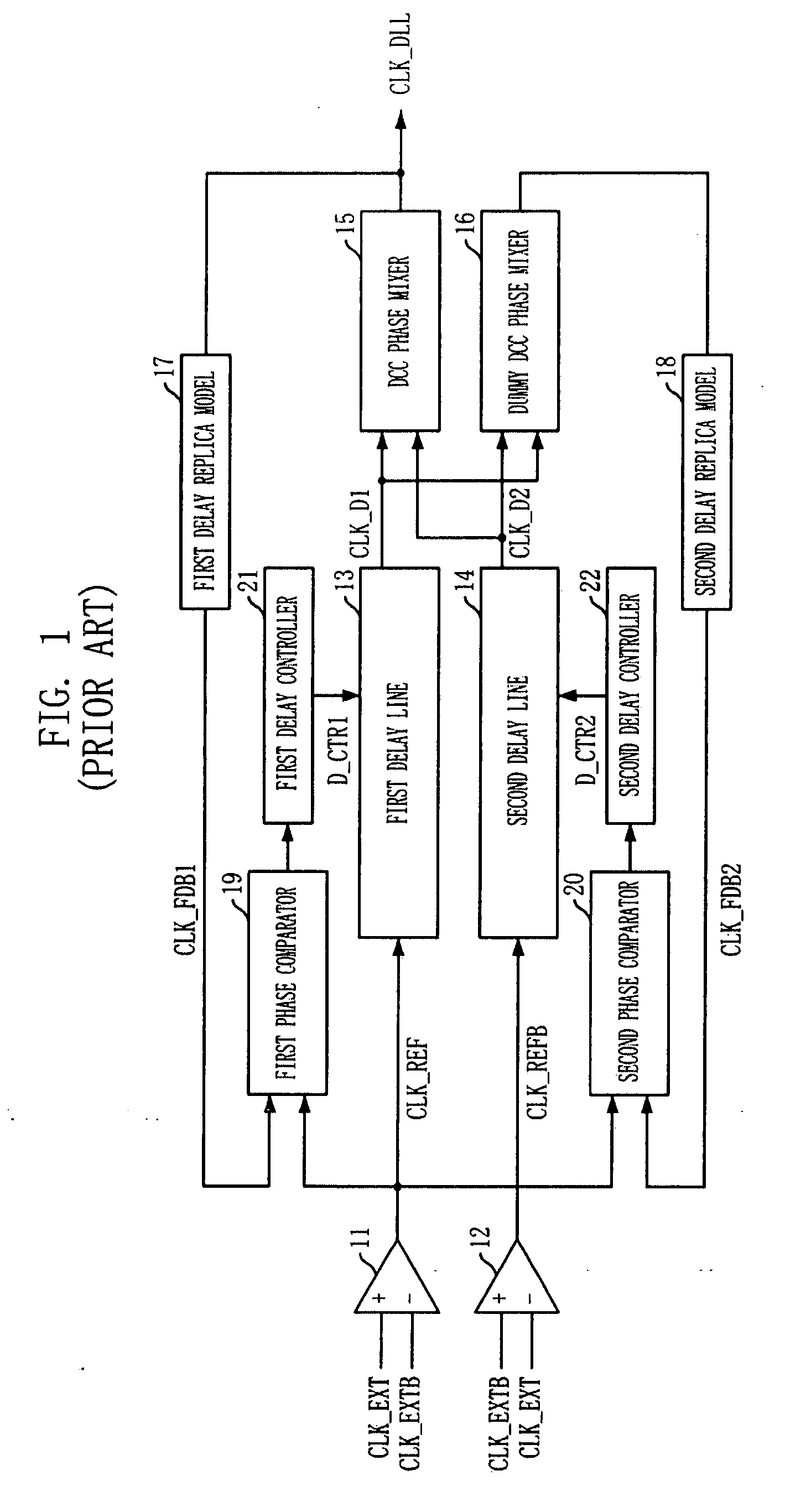
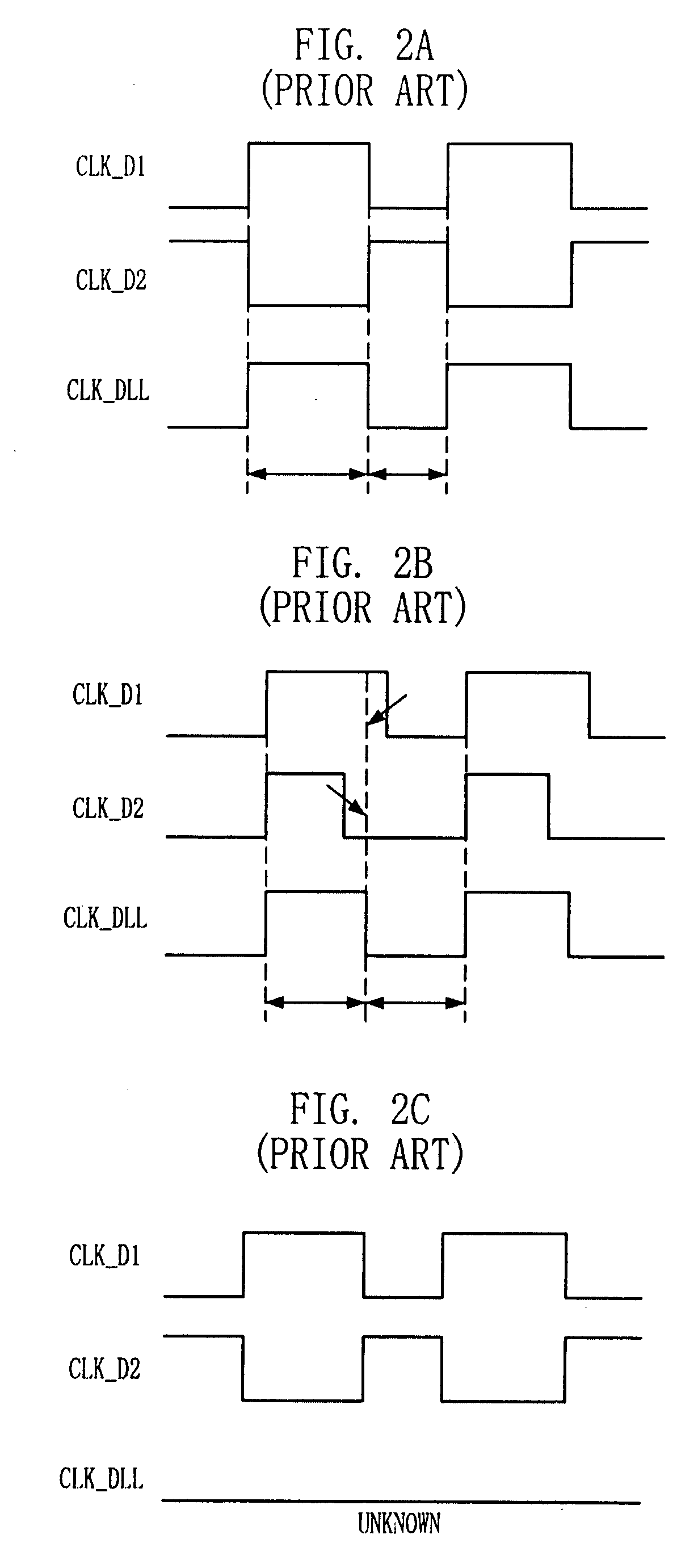
[0033]The DLL in accordance with the embodiment of the present invention is different from the conventional DLL of FIG. 1 in that the DCC controller 500 is further included, but the first and second clock buffers 11 and 12, the first and second delay replica models 17 and 18, the first and second phase comparators 19 and 20, and the first and second delay controllers 21 and 22 are omitted. Further, the technical implementation and operation of the first and second delay lines 100 and 200 are substantially equal ...


PUM


Abstract

A delay locked loop (DLL) of a semiconductor device includes: a first delay line for delaying a first clock signal in synchronization with a first edge of an external clock signal to output a first delayed clock signal; a second delay line for delaying a second clock signal in synchronization with a second edge of the external clock to output a second delayed clock signal; a duty cycle corrector (DCC) for mixing phases of the first and second delayed clock signals to output a DLL clock signal with a corrected duty cycle; and a DCC controller for disabling the duty cycle corrector in a section during which a phase difference between the first and second delayed clock signals is greater than a preset time after a delay locking.

Description

CROSS-REFERENCE TO RELATED APPLICATIONS[0001]The present invention claims priority of Korean patent application number 10-2006-106765, filed on Oct. 31, 2006, which is incorporated by reference in its entirety.BACKGROUND OF THE INVENTION[0002]The present invention relates to a semiconductor device, and more particularly, to a delay locked loop (DLL) having a duty cycle corrector (DCC).[0003]In synchronous semiconductor memory devices such as a double data rate (DDR) synchronous dynamic random access memory (SDRAM), data are transferred to other devices in synchronization with a DLL clock signal (CLK_DLL) generated by delaying an external clock signal (CLK_EXT) inputted from an external circuit such as a memory controller. Examples of a clock synchronization circuit include a phase locked loop (PLL) and a delay locked loop (DLL). The DLL is widely used in semiconductor devices because it has low noise and can be implemented in a small area compared with the PLL.[0004]The trend of the...

Claims


Application Information

Patent Timeline
Patent Type & Authority Applications(United States)
IPC IPC(8): H03L7/06H03K3/017
CPCH03L7/095H03L7/0812G11C11/4076G11C2207/2254H03K5/1565
Inventor LEE, HYE-YOUNG
Owner SK HYNIX INC
Why Eureka
Try Eureka