III-Nitride wafer fabrication

a technology of iii-nitride and fabrication process, which is applied in the direction of semiconductor/solid-state device manufacturing, basic electric elements, electric apparatus, etc., can solve the problems of only accumulating stress in the iii-nitride film, warpage and defects of the wafer, and the cracking of the epitaxial film, so as to reduce the total stress buildup across the wafer and reduce the overall stress. , the effect of reducing warpag

Active Publication Date: 2008-05-01
INFINEON TECH AMERICAS CORP
View PDF19 Cites 10 Cited by
  • Summary
  • Abstract
  • Description
  • Claims
  • Application Information

AI Technical Summary

Benefits of technology

[0006] To reduce warpage and defects, according to the present invention, an array or grid of “control joints” is fabricated onto a surface of a substrate before epitaxial growth of a III-nitride film, such that the epitaxial film is discontinuous across the control joints. As a result, stresses in the III-nitride film are only able to accumulate inside the boundaries defined by the control joints and cannot propagate past the control joints. The control joints also may force an intentional “crack” in the III-nitride film, localized near the control joint, which can lower the total stress buildup across the wafer, resulting in lower overall wafer warpage.

Problems solved by technology

The wafer warpage, epitaxial film cracks, and defects can occur from the cumulative stress buildup over the surface of a whole wafer.
As a result, stresses in the III-nitride film are only able to accumulate inside the boundaries defined by the control joints and cannot propagate past the control joints.
The control joints also may force an intentional “crack” in the III-nitride film, localized near the control joint, which can lower the total stress buildup across the wafer, resulting in lower overall wafer warpage.

Method used


Image

  • III-Nitride wafer fabrication
  • III-Nitride wafer fabrication
  • III-Nitride wafer fabrication

Examples


Embodiment Construction

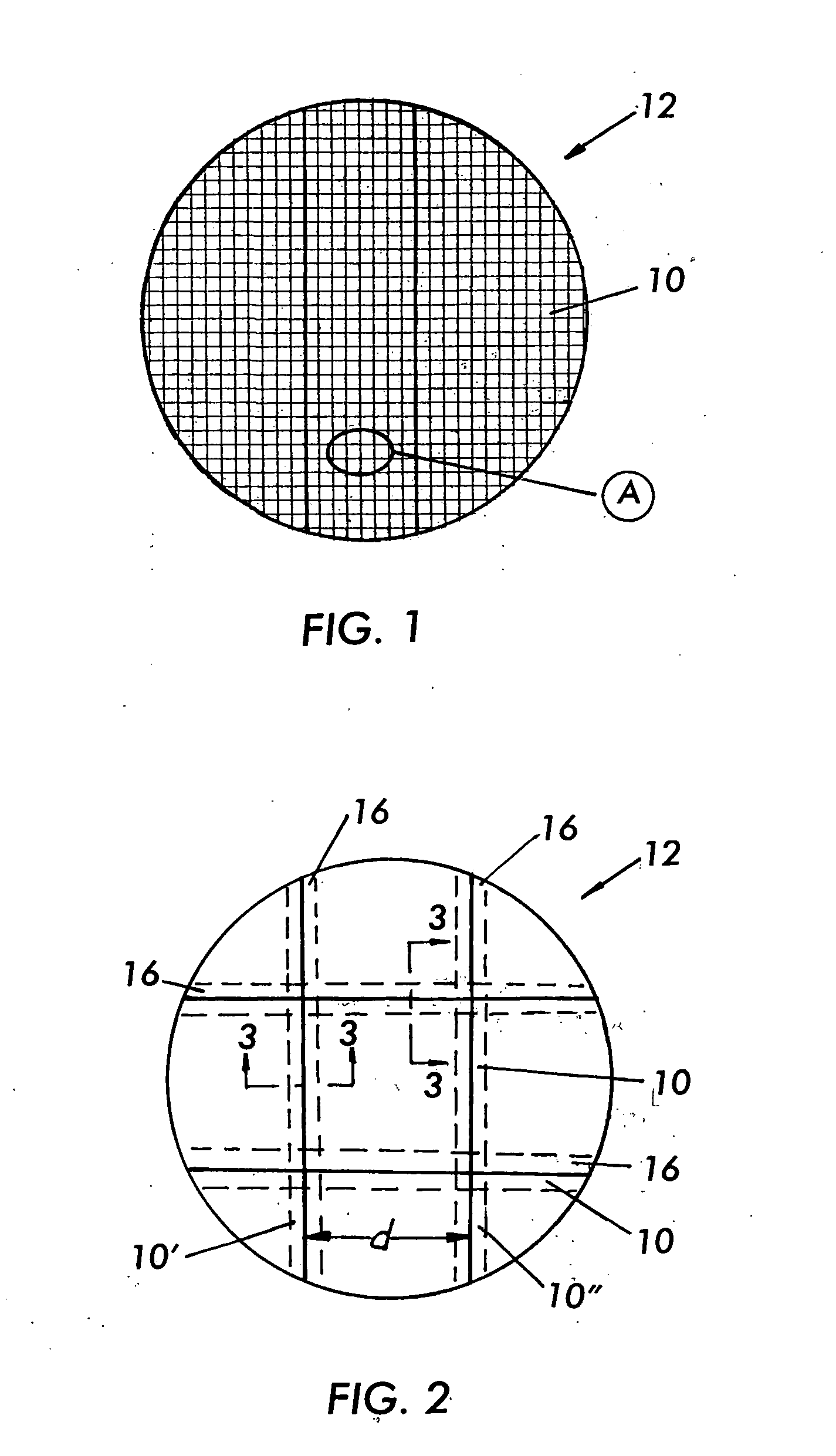
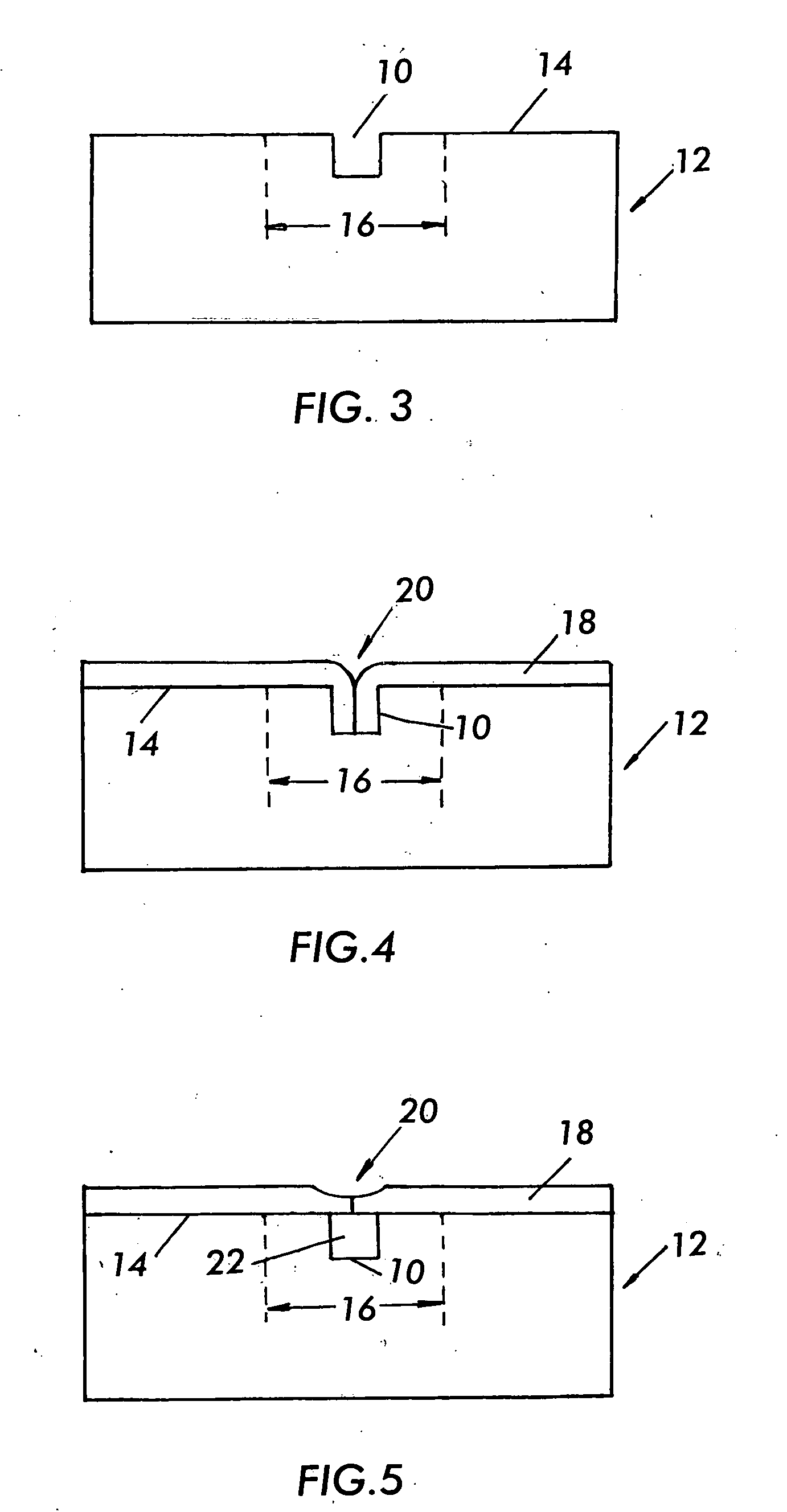
[0017] Referring to FIGS. 1, 2, and 3, in a method according to one embodiment of the present invention shallow trenches 10 are etched into one surface of a silicon wafer 12. Preferably, trenches 10 cross one another to form a grid, as specifically illustrated by FIGS. 1 and 2. Trenches 10 function to reduce the overall stress in the III-nitride epitaxial layer that is to be formed over surface 14 of wafer 12. Each trench 10 may be about 100 angstroms deep, and several microns wide. Furthermore, the center-to-center spacing d of opposing trenches (e.g. trenches 10′ and 10″) may be in the range of 10-25 mm.

[0018] According to one aspect of the present invention trenches 10 are formed inside regions 16 of wafer 12 designated as saw street for the dicing of the wafer into individual die.

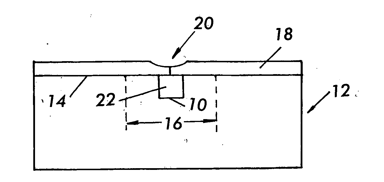
[0019] Referring now to FIG. 4, according to the present invention, a III-nitride body 18 (e.g. AlN) is epitaxially formed over surface 14 of wafer 12 and filling trenches 10. Note that film 18 is ren...


PUM


Abstract

A method for fabrication of a III-nitride film over a silicon wafer that includes forming control joints to allow for overall stress relief in the III-nitride film during the growth thereof.

Description

RELATED APPLICATION [0001] This application is based on and claims priority to the U.S. Provisional Application Ser. No. 60 / 863,427, filed on Oct. 30, 2006, entitled III-Nitride Global Stress Reduction, to which a claim of priority is hereby made and the disclosure of which is incorporated by reference.DEFINITION [0002] III-nitride as set forth herein refers to an alloy from the InAlGaN system including but not limited to AlN, AlGaN, GaN, InGaN, InN, InAlGaN or the like. FIELD OF THE INVENTION [0003] The present invention relates to semiconductor device fabrication and particularly to the fabrication of wafers for III-nitride semiconductor devices. BACKGROUND OF THE INVENTION [0004] Epitaxial growth or deposition of III-nitride films onto substrates of a different material (e.g. silicon) often results in high epitaxial defect density, high film stresses, high wafer warpage, and cracks in the epitaxial films, which are typically caused by the large lattice constant mismatch between t...

Claims


Application Information

Patent Timeline
Patent Type & Authority Applications(United States)
IPC IPC(8): H01L21/76
CPCH01L21/02381H01L21/0243H01L21/78H01L21/02494H01L21/0254H01L21/02488
Inventor HERMAN, THOMASBEACH, ROBERT
Owner INFINEON TECH AMERICAS CORP
Why Eureka
Try Eureka