Integrated circuit interconnect lines having reduced line resistance

Inactive Publication Date: 2008-05-08
APPLIED MATERIALS INC
View PDF0 Cites 0 Cited by
  • Summary
  • Abstract
  • Description
  • Claims
  • Application Information

AI Technical Summary

Benefits of technology

[0011]An interconnect line trench design is prepared in the third dielectric layer wherein the line trench design crosses over the at least two dense lines. One or more dense line subsets are formed in the first dielectric layer such that the one or more dense line subsets underlay the trench design.
[0012]A first etch mask layer is deposited on the dielectric stack. Thereafter, the mask layer is developed to form etch masks that underlay the trench design but do not extend to the full length of the trench design. The etch masks do not cross over the underlying one or more dense line subsets. The etch masks are then used for etching slots through the second and third dielectric layers such that each slot is positioned at a novel tolerance space di

Problems solved by technology

Mask writing usually requires a significant write-time due to the complexities, such as optical proximity correction (OPC), and the volume of the fractured data.

Method used


Image

  • Integrated circuit interconnect lines having reduced line resistance
  • Integrated circuit interconnect lines having reduced line resistance
  • Integrated circuit interconnect lines having reduced line resistance

Examples


Embodiment Construction

[0035]While describing the invention and its embodiments, certain terminology will be utilized for the sake of clarity. It is intended that such terminology includes the recited embodiments as well as all equivalents.

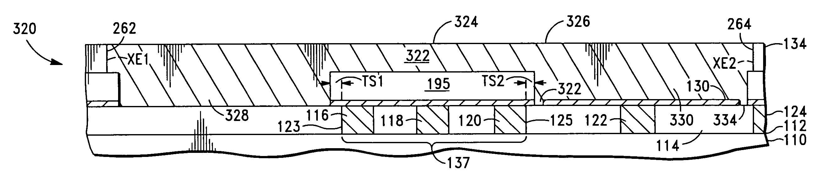
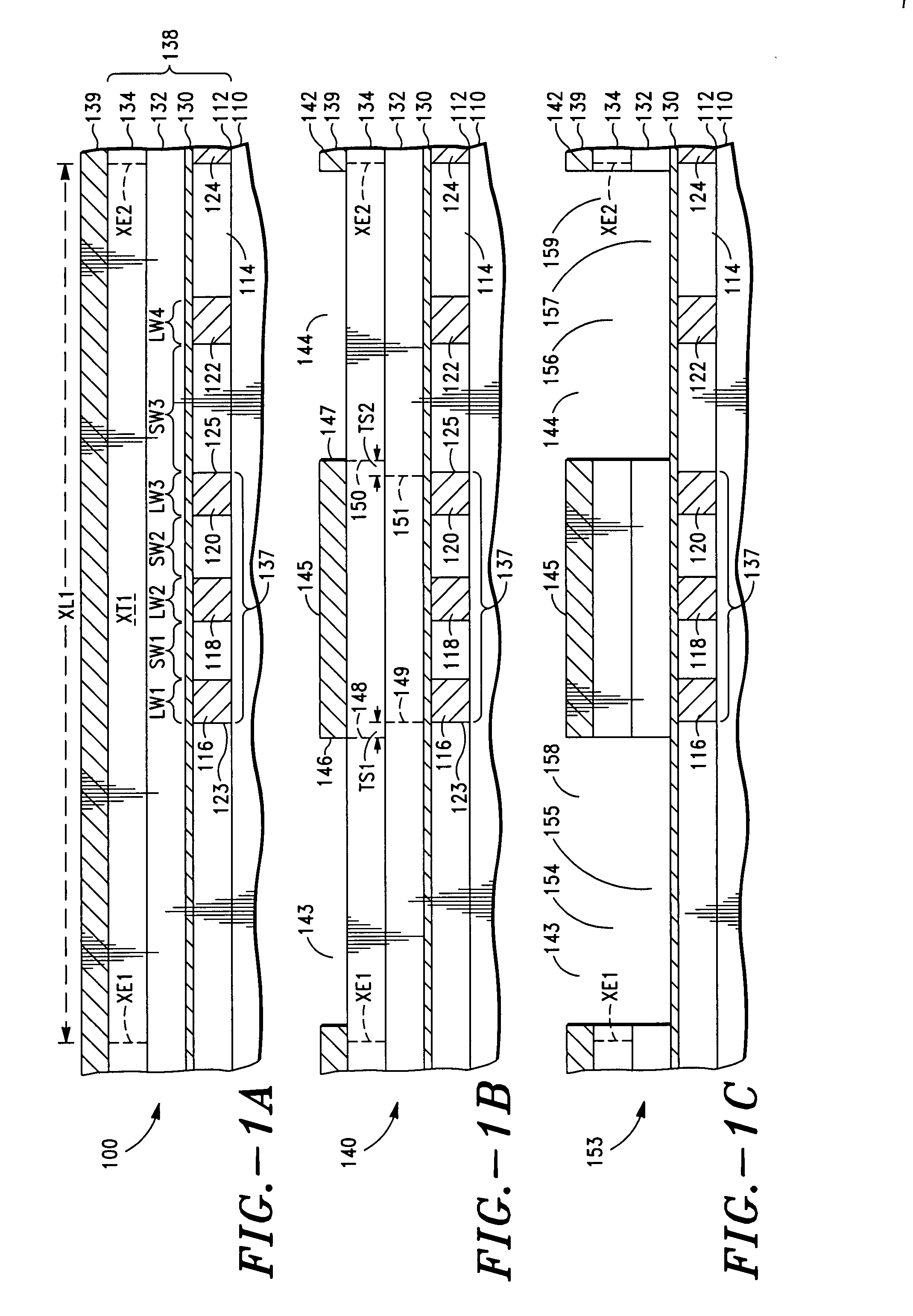
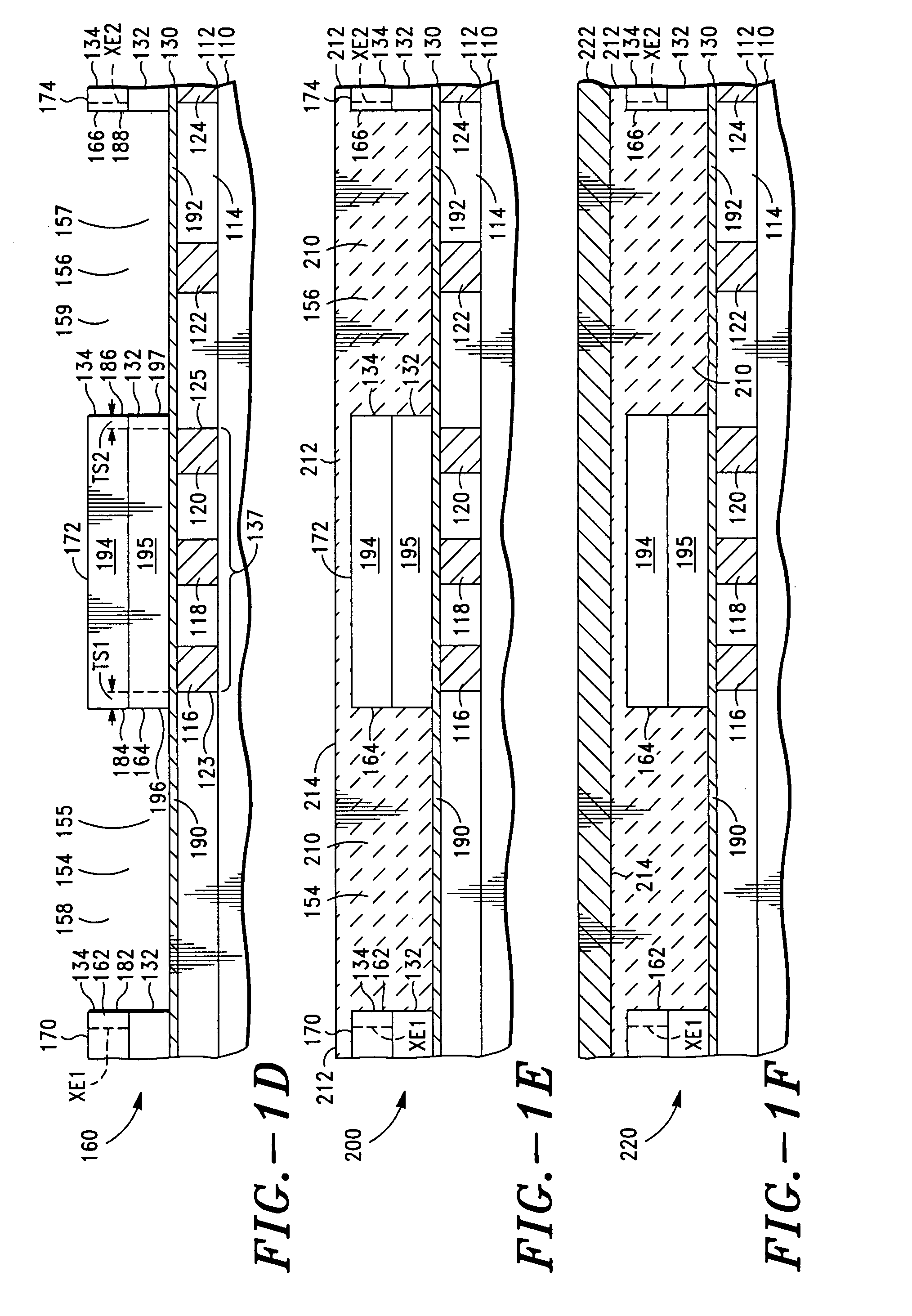
[0036]One embodiment of the invention, schematically illustrated in FIGS. 1A-1V, shows a novel processing sequence, for forming IC structures including IC structures comprising an interconnect line having electrically conductive shunts that are in alignment with the interconnect line. The expression “integrated circuit structure” as defined herein, means completely formed integrated circuits and partially formed integrated circuits.

[0037]FIG. 1A shows an IC structure 100 having a semiconductor substrate 110, including a substrate top surface 112. The expression “semiconductor substrate” as defined herein, means structures and devices comprising typical IC elements, components, interconnects and semiconductor materials. A first dielectric layer 114 is formed on top surfa...


PUM


Abstract

The present invention provides integrated circuit fabrication methods and devices wherein shunted interconnect lines are formed. The shunted interconnect lines are formed in a dielectric stack comprising (1) a first dielectric layer having dense interconnect lines that form a first dielectric layer dense line subset and (2) a sequentially deposited (i) etch stop layer, (ii) second dielectric layer and (iii) third dielectric layer. An interconnect line trench design is prepared in the third dielectric layer. An interconnect line trench is formed in the third dielectric layer according to the interconnect line trench design. One or more electrically conductive shunts are fabricated in the second dielectric layer such that the one or more shunts (1) extend from the interconnect line trench to the etch stop layer and (2) do not cross over the first dielectric layer dense line subset.

Description

FIELD OF THE INVENTION[0001]The present invention relates to integrated circuit (IC) interconnect lines employing electrically conductive interconnect line shunts for reduced resistance of interconnect lines.BACKGROUND OF THE INVENTION[0002]A typical integrated circuit chip layout is prepared by employing a CAD (computer-aided design) tool to place and route cells from a library of cells and custom circuit blocks to form a complete chip layout. The internal layout data base is converted to a standard stream file format such as GDS-II, for mask making. GDS-II is available from Cadence Design Systems, located in San Jose, Calif. An electronic design automation (EDA) tool can be employed for creating the schematic circuit design. EDA tools are available from Cadence Design Systems.[0003]Typically, an IC chip includes a semiconductor substrate and several layers that are sequentially deposited on the substrate. The CAD layout that includes the IC elements, including the library cells of...

Claims


Application Information

Patent Timeline
IPC IPC(8): H01L23/12
CPCH01L23/5222H01L23/53238H01L23/53295H01L2924/0002H01L2924/00H01L23/5221H01L23/5283
Inventor PARIKH, SUKETU A.
Owner APPLIED MATERIALS INC
Why Eureka
Try Eureka