Epitaxial solid-state semiconducting heterostructures and method for making same

Inactive Publication Date: 2010-11-18
CENT NAT DE LA RECHERCHE SCI
View PDF18 Cites 0 Cited by
  • Summary
  • Abstract
  • Description
  • Claims
  • Application Information

AI Technical Summary

Benefits of technology

[0017]From a fundamental point of view, it is assumed that this result is linked to the crystallographic and chemical heterogeneity between the epitaxial semiconductor on the crystalline oxide and the oxide itself. This heterogeneity makes it possible to avoid deformation of the semiconductor during the first stages of growth, which is at the origin of the formation of defects as described in the introduction, to the advantage of the deformation or rupture of interface bonds.
[0097]It also permits the integration, on a monocrystalline oxide layer on a substrate, of semiconducting quantum dots which are unstrained, that is to say have their bulk lattice parameter, and allows their shape, their size and their density to be controlled without any limitation associated with the strain between the semiconductor and the oxide or the substrate.

Problems solved by technology

Such techniques involve complex technologies and are very expensive.
However, heteroepitaxy processes are at present limited by the difficulties arising from the parametric mismatch between the substrate and the material to be deposited by epitaxy.
This transformation is accompanied by the formation of structural defects (dislocations, twins, stacking faults) which render the material unfit for use for the intended applications.
This approach also has limits, however.
On the other hand, it is specific to GaAs and cannot be considered for other materials such as InP, which is a leading semiconductor for optoelectronic applications in the infrared range,
However, it is highly probable that the dilatation of the lattice parameter induced by annealing is accompanied by an undulation of the layers, which is highly detrimental to the crystalline quality of the GaAs taken up on the oxide.
In addition, this approach has not hitherto been practised on an industrial scale.

Method used


Image

  • Epitaxial solid-state semiconducting heterostructures and method for making same
  • Epitaxial solid-state semiconducting heterostructures and method for making same
  • Epitaxial solid-state semiconducting heterostructures and method for making same

Examples


example 1

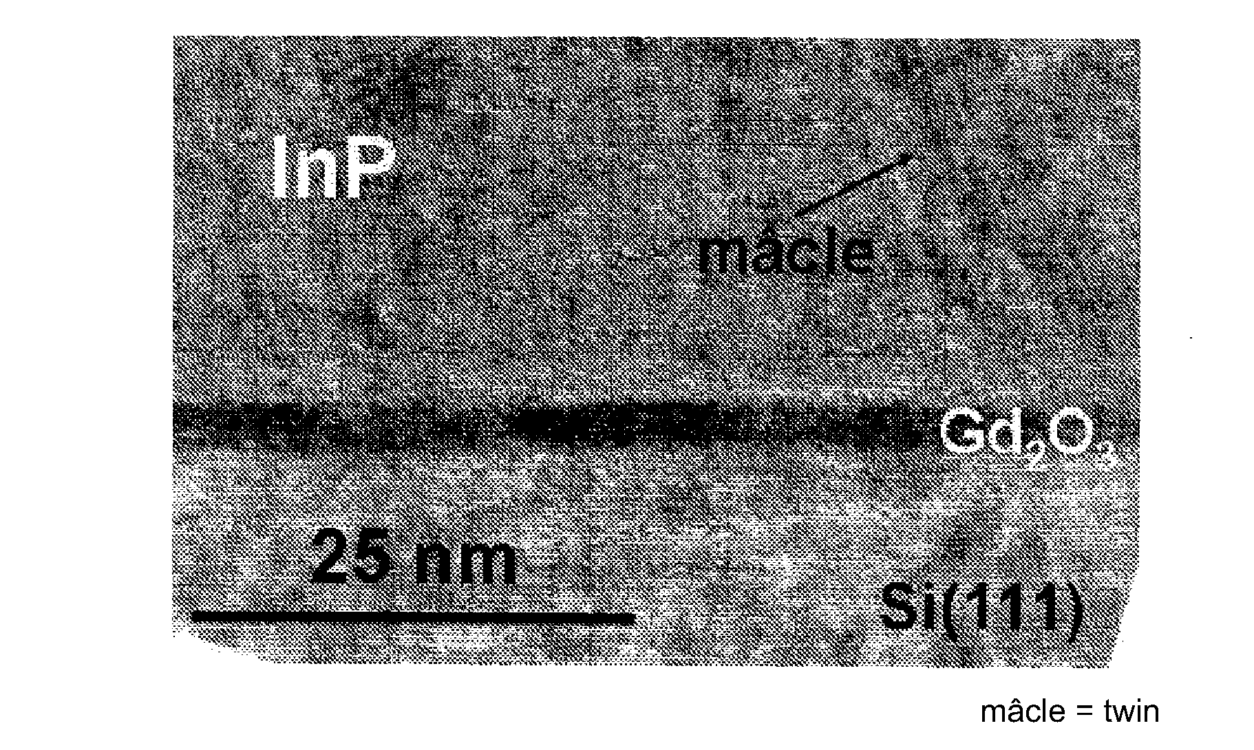
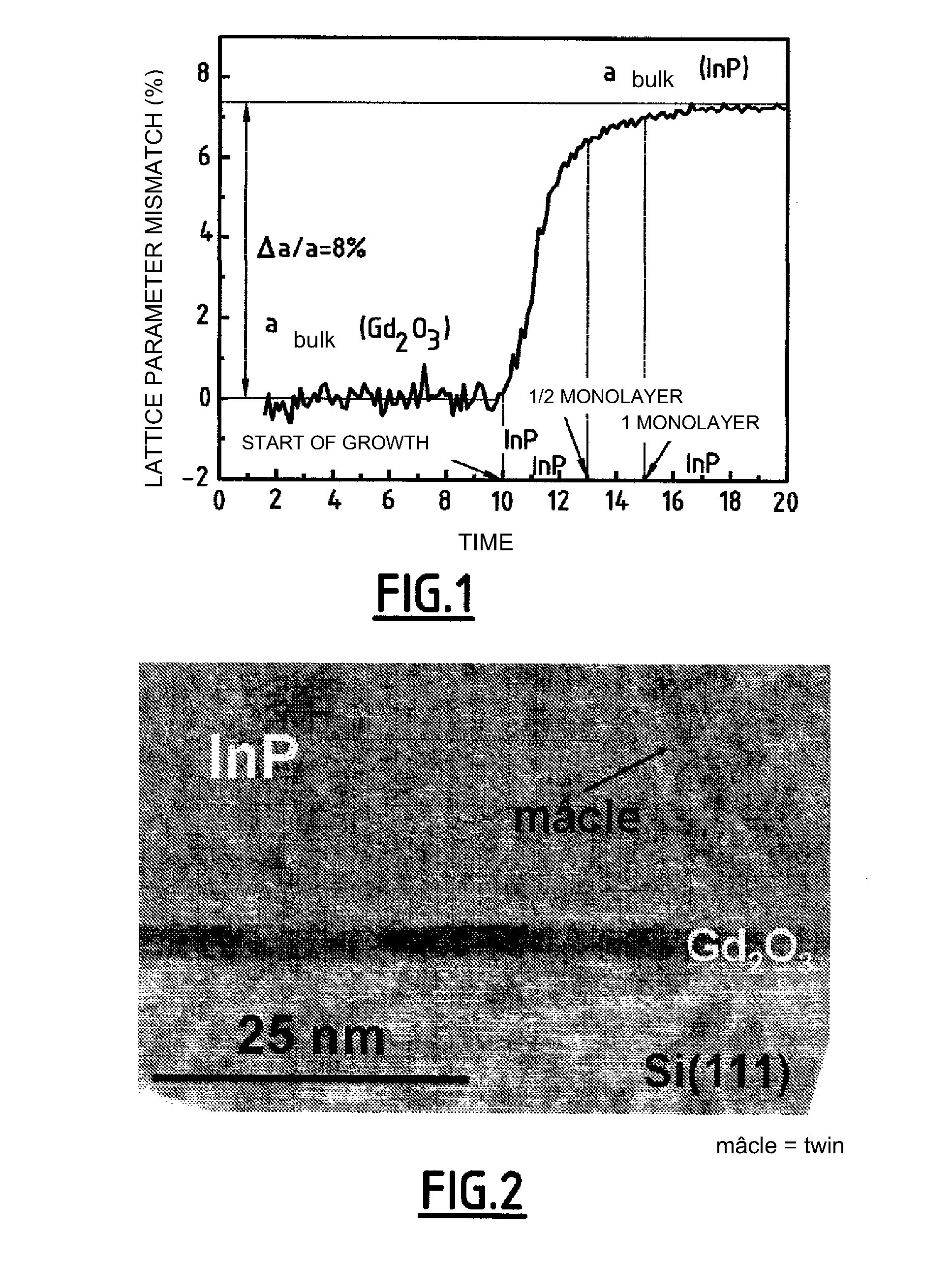
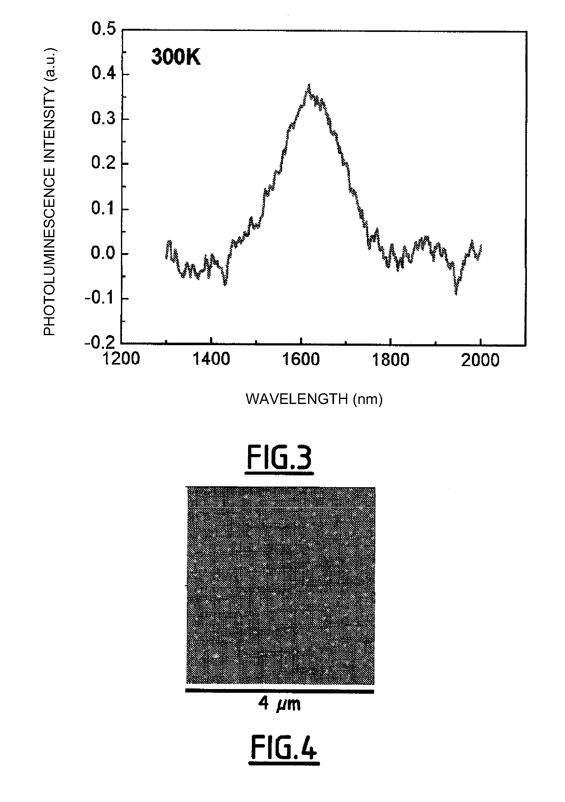
[0105]Preparation of a Semiconducting Heterostructure (InAsP,InP) / Gd2O3 / Si111

[0106]An Si(111) substrate (obtainable from ACM, France) is subjected to cleaning comprising immersion for 10 seconds in a bath of pure NI4F followed by rinsing with deionized water and drying, before it is immediately introduced into a modified RIBER 2300 chamber for the growth of oxides by molecular beam epitaxy.

[0107]A thickness of 4 nm of Gd2O3 is deposited on the substrate by evaporating a Gd2O3 target by means of an electron gun at a temperature of 700° C., a partial oxygen pressure of 10−6 torr being adjusted. A strained monocrystalline Gd2O3 layer of excellent quality is obtained.

[0108]The substrate so coated is then removed from the RIBER 2300 chamber and introduced into a connected system, under an ultrahigh vacuum, comprising a chamber for cleaning under O2 and a molecular beam epitaxy device (RIBER 32 chamber). Treatment under molecular oxygen (pressure 10−5 torr) is carried out in the cleaning ...

example 2

[0121]Preparation of a semiconducting heterostructure InP / SrTiO3 / Si(001)

[0122]A layer of SrTiO3 is deposited by molecular beam epitaxy in a RIBER 2300 chamber on an Si(001) substrate supplied by STMicroelectronics and previously cleaned as in Example 1.

[0123]The surface of the Si is first treated by forming a monolayer of SrO. To that end, the temperature of the substrate is brought to 550° C. and its surface is exposed to a strontium pressure of 5.10−8 torr for 3 minutes. The substrate is then brought to 750° C., which causes the stabilization of ⅓ of a monolayer of Sr at the surface of the silicon. The temperature of the substrate is then brought to 550° C. again, and the substrate is exposed to the same flow of strontium until ½ monolayer is obtained. Finally, the temperature of the substrate is brought to the growth temperature of SrTiO3 (from 350 to 400° C.), and the surface is exposed to a partial oxygen pressure of 5.10−8 torr in order to oxidize the ½ monolayer of strontium ...


PUM


Abstract

A method for producing a solid-state semiconducting structure, includes steps in which:(i) a monocrystalline substrate is provided;(ii) a monocrystalline oxide layer is formed, by epitaxial growth, on the substrate;(iii) a bonding layer is formed by steps in which:(a) the impurities are removed from the surface of the monocrystalline oxide layer;(b) a semiconducting bonding layer is deposited by slow epitaxial growth; and(iv) a monocrystalline semiconducting layer is formed, by epitaxial growth, on the bonding layer so formed. The solid-state semiconducting heterostructures so obtained are also described.

Description

FIELD OF THE INVENTION[0001]The present invention relates to epitaxial solid-state semiconducting heterostructures and to a method for producing them.PRIOR ART[0002]The integration of optoelectronic components into silicon-based systems is a key point in the development of the performances of such systems.[0003]The most mature methods for integrating semiconductors on silicon, such as vignetting, smartcut or wafer bonding, are based on techniques of transfer by adhesive bonding. Such techniques involve complex technologies and are very expensive.[0004]The production of solid-state semiconducting heterostructures by epitaxy would allow the technological complexity of the methods, and consequently the production costs, to be reduced considerably.[0005]However, heteroepitaxy processes are at present limited by the difficulties arising from the parametric mismatch between the substrate and the material to be deposited by epitaxy. The first monolayers of a material with lattice mismatch ...

Claims


Application Information

Patent Timeline
IPC IPC(8): H01L29/267H01L21/20H01L29/04
CPCH01L21/02381H01L21/02433H01L21/02488H01L21/02546H01L21/02532H01L21/02543H01L21/02502
Inventor SAINT-GIRONS, GUILLAUMELARGEAU, LUDOVICPATRIARCHE, GILLESREGRENY, PHILIPPEHOLLINGER, GUY
Owner CENT NAT DE LA RECHERCHE SCI
Why Eureka
Try Eureka