Semiconductor Single Crystal Production Device And Producing Method Therefor

a production device and single crystal technology, applied in the direction of crystal growth process, crystal growth process, polycrystalline material growth, etc., can solve the problems of changing the temperature distribution of the melt b>4/b>, badly affecting the quality of the single crystal, etc., to achieve stably pulled up and produced, high quality single crystal, and prolong the useful life of the employed parts

Active Publication Date: 2008-05-15
SUMCO TECHXIV
View PDF15 Cites 12 Cited by
  • Summary
  • Abstract
  • Description
  • Claims
  • Application Information

AI Technical Summary

Benefits of technology

[0039]In addition, according to the semiconductor single crystal producing method of the present invention, because the change of thermal expansion coefficient in the heat shield 12 can be suppressed and the distance between the lower end position of the radiation screen 10 and the melt

Problems solved by technology

As a result, the temperature distribution of the melt 4 is changed to badly affect the

Method used


Image

  • Semiconductor Single Crystal Production Device And Producing Method Therefor
  • Semiconductor Single Crystal Production Device And Producing Method Therefor
  • Semiconductor Single Crystal Production Device And Producing Method Therefor

Examples


Embodiment Construction

[0040]Embodiments of a semiconductor single crystal production device according to the present invention are described with reference to the drawings.

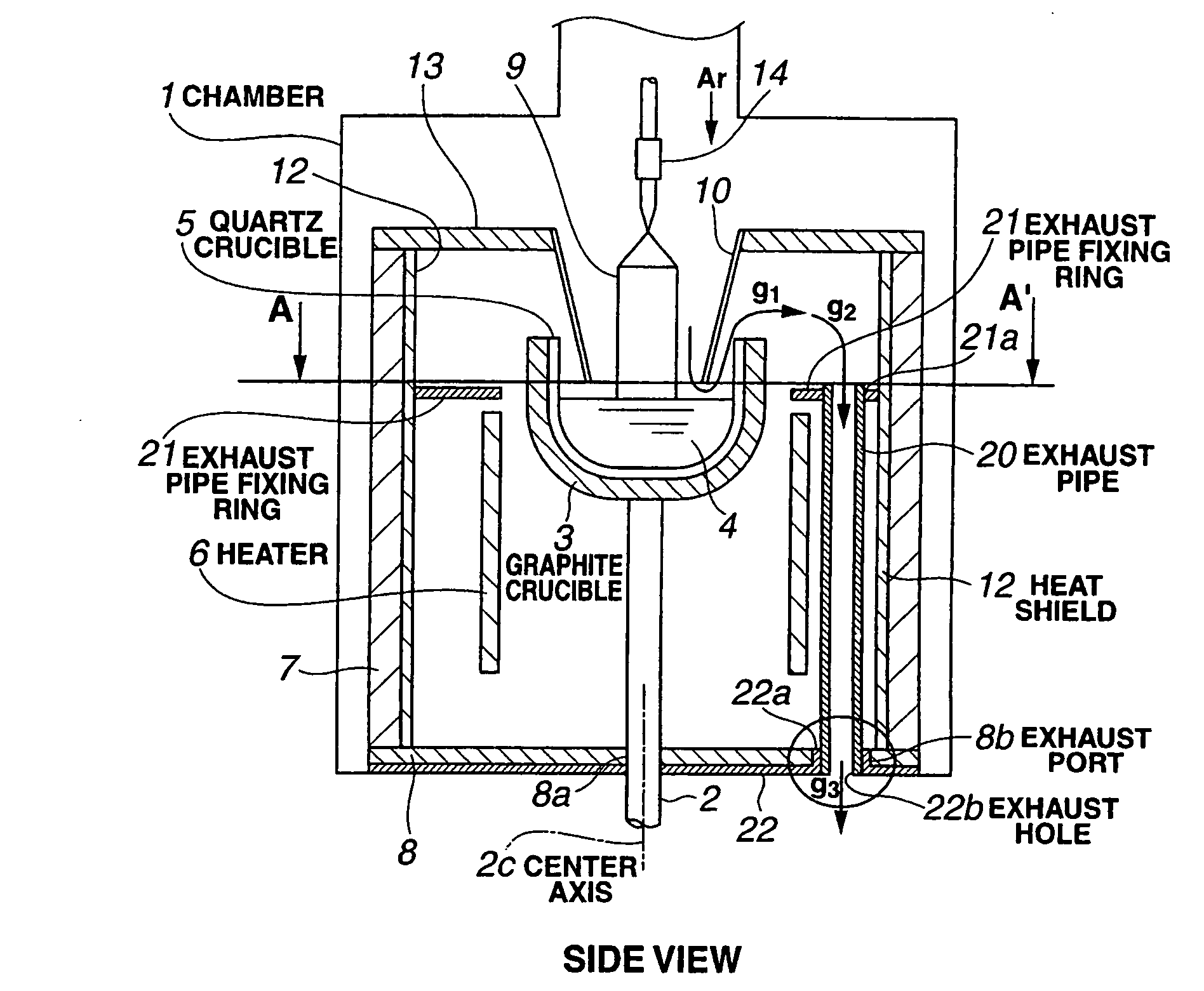
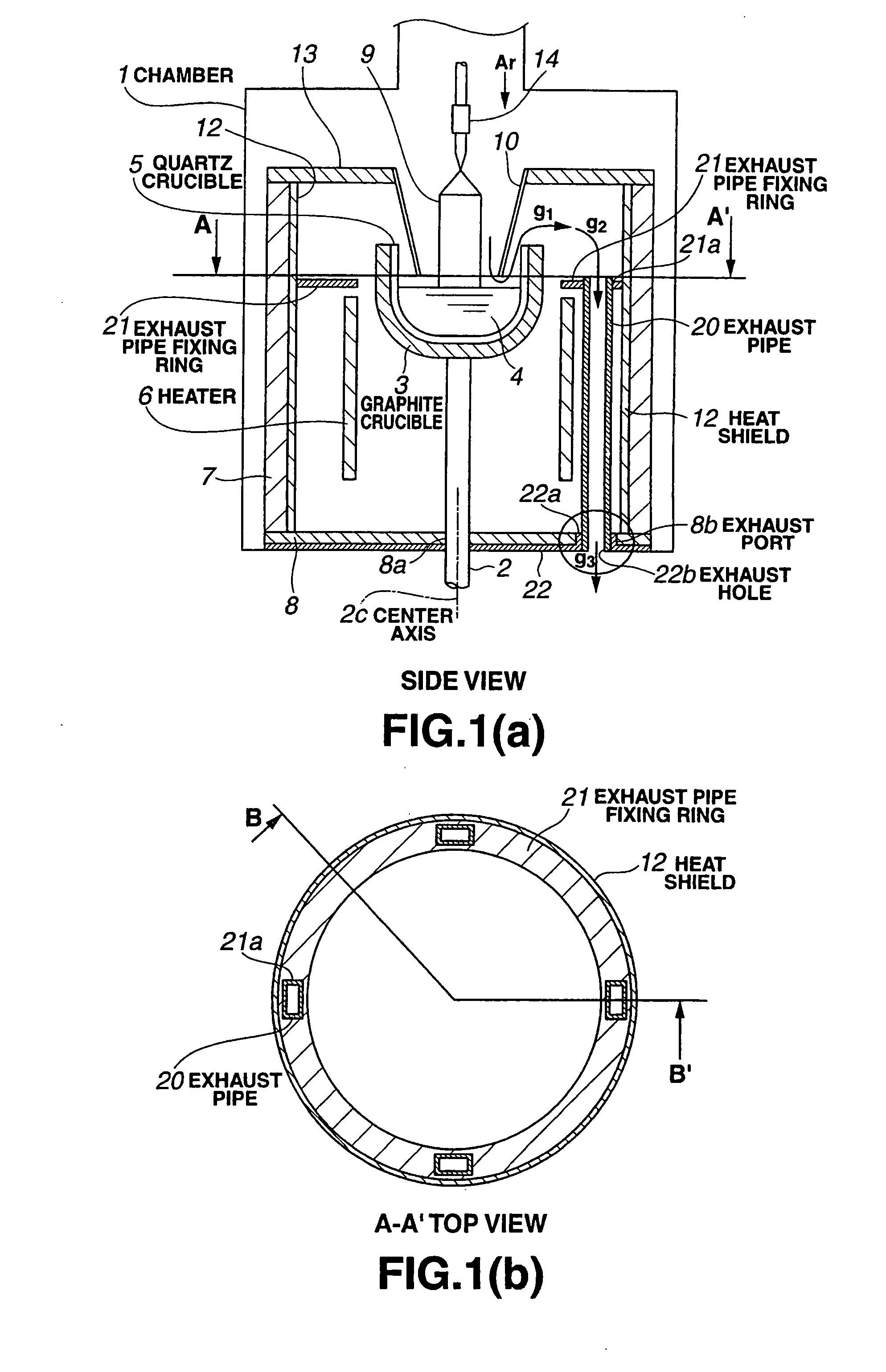
[0041]FIG. 1 shows a configuration of a silicon single crystal production device of an embodiment according to the present invention in a cross-section.

[0042]FIG. 1(a) is a side view and FIG. 1(B) is a top view. The A-A′ cross-section in FIG. 1(a) is equivalent to the top view of FIG. 1(B) and the B-B′ cross-section in FIG. 1(B) is equivalent to the side view of FIG. 1(a).

[0043]As shown in these views of FIG. 1, a crucible axis 2 is provided at the center of a chamber 1. The center axis of the crucible axis 2 is equivalent to that of the chamber 1. An upper end of the crucible axis 2 supports a graphite crucible 3 through an unillustrated crucible receiver.

[0044]A quartz crucible 5 is accommodated in the graphite crucible 3. The quartz crucible 5 contains a melt 4.

[0045]A cylindrical heater 6 is provided outside the graphite crucible 3...


PUM


Abstract

Evaporated matters and reaction products produced in a furnace can be exhausted without contacting with a graphite crucible and a heater, and an exhaust pipe per se can be maintained at a high temperature to suppress the deposition and condensation of the evaporated matters and reaction products, whereby the clogging of the exhaust pipe is prevented, in addition, a conversion of the exhaust pipes per se into SiC is suppressed to improve the durability of the exhaust pipe, and the change in thermal expansion coefficient is suppressed, whereby a thermal single crystal can be pulled up in high quality. Further, the exhaust pipe is formed of a small number of materials to reduce a production cost. A heat shield (12) made of a heat insulating material is provided outside a heater (6), and a plurality of exhaust pipes (20) are provided between the heater (6) and the heat shield (12). The plurality of exhaust pipes (20) are communicated with a plurality of exhaust ports (8B (22b)) provided at a bottom of a chamber 1.

Description

TECHNICAL FIELD[0001]The present invention relates to a semiconductor single crystal production device and a producing method therefor.BACKGROUND ART[0002]A high-purity silicon single crystal is mainly used for the substrate of a semiconductor device. As one of the methods for producing the silicon single crystal, Czochralski process (referred to as “CZ process”) is provided. In the CZ process, as one example as shown in FIG. 8, a silicon polycrystal is filled in a quartz crucible 5 disposed in a chamber 1 of a semiconductor single crystal production device, the silicon polycrystal is heated and melted into a melt 4 by a heater 6 provided around the quartz crucible 5, then a seed crystal attached to a seed chuck 14 is immersed into the melt 4, and the seed chuck 14 is pulled up while rotating the seed chuck 14 and the quartz crucible 5 in the same direction or a reverse direction, whereby the silicon single crystal 9 is grown. In addition, in FIG. 8, a heat insulating cylinder 7 is ...

Claims


Application Information

Patent Timeline
IPC IPC(8): C30B23/00C30B11/00
CPCC30B15/00C30B15/10C30B15/14Y10T117/1052Y10T117/10Y10T117/106Y10T117/108C30B29/06H01L21/20H01L29/04
Inventor NODA, AKIKOIIDA, TETUHIRO
Owner SUMCO TECHXIV
Why Eureka
Try Eureka