

Semiconductor device and method for manufacturing the same
- Summary
- Abstract
- Description
- Claims
- Application Information
AI Technical Summary
Benefits of technology
Problems solved by technology
Method used
Image

Examples
embodiment mode 1
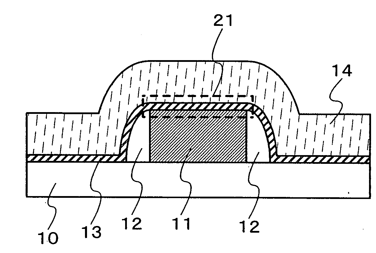
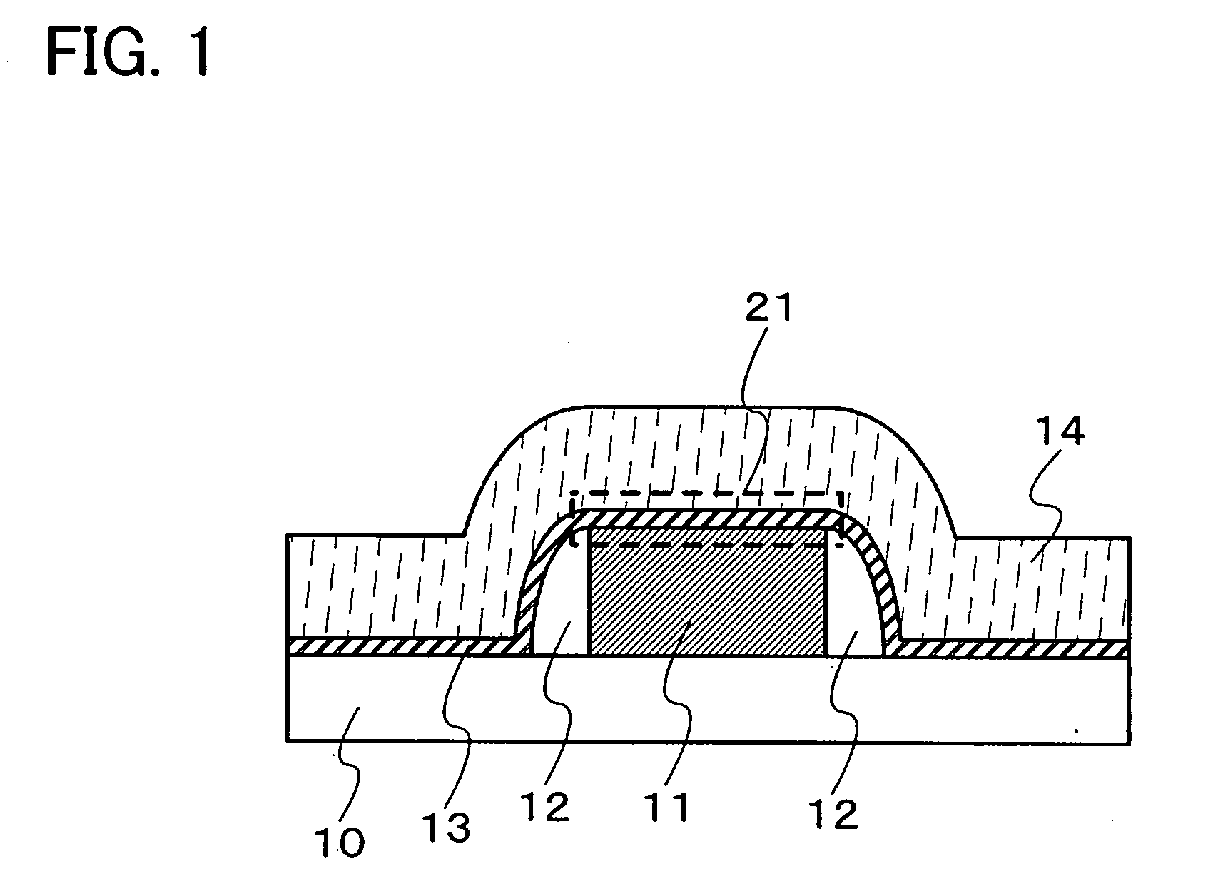
[0040]In this embodiment mode, a structure of a memory element having an insulating material on a side surface of a conductive layer serving as a cathode or anode will be described.
[0041]As shown in FIG. 1, the memory element in this embodiment mode includes a first electrode 11 formed over a substrate 10 which has a insulating surface, a sidewall insulating layer 12 formed on a side surface of the first electrode 11, a silicon film 13 formed to cover the first electrode 11 and the sidewall insulating layer 12, and a second electrode 14 formed over the silicon film 13. Note that a step portion is formed by the substrate 10 and the first electrode 11, and the silicon film 13 and the second electrode 14 are formed to cover the step portion. In addition, the sidewall insulating layer 12 prevents the side surface of the first electrode 11 and the silicon film 13 from directly touching each other. A surface of the sidewall insulating layer 12 touching the silicon film 13 may be curved. W...
embodiment mode 2
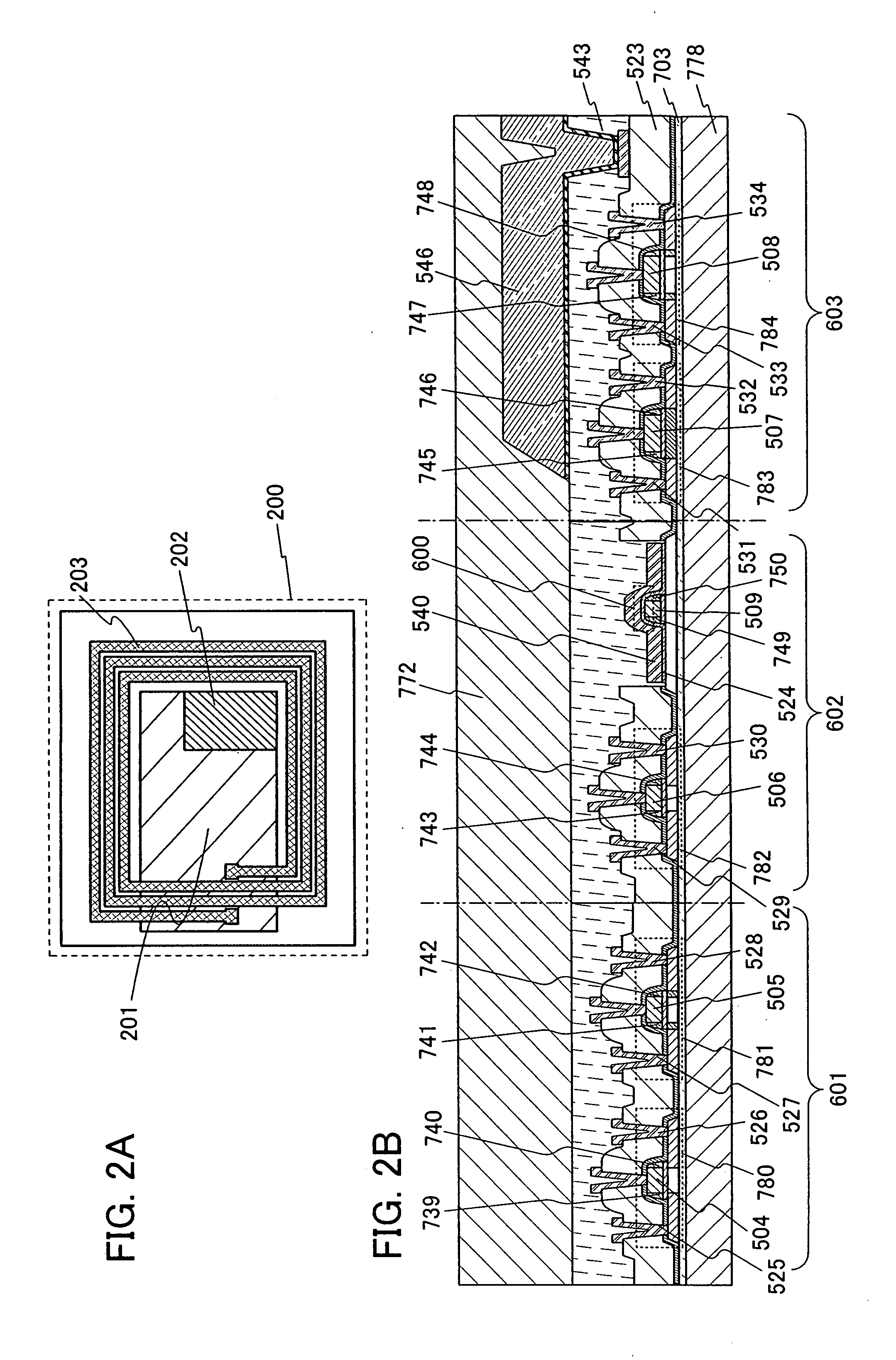
[0056]In this embodiment mode, steps for manufacturing the semiconductor device including the memory elements shown in Embodiment Mode 1 will be described with reference to the drawings. A wireless chip capable of wireless communication with outside as an example of the semiconductor device including the memory elements will be described in this embodiment mode.
[0057]First, a separation layer 702 is formed over one surface of a first substrate 701 (FIG. 3A). When the first substrate 701 has an insulating surface, there is no particular limitation on the first substrate 701. For example, a substrate such as a quartz substrate, a glass substrate, or a plastic substrate can be used. If the first substrate 701 is formed of glass, there are no particular limitations on the area and the shape thereof. Thus, for example, when a substrate having one side of one meter or longer and rectangular shape is used for the first substrate 701, the productivity can be drastically improved. Such advan...
embodiment mode 3
[0110]A structural example of the semiconductor device employing the present invention will be described with reference to FIG. 9. As shown in FIG. 9, a semiconductor device 1520 of the present invention has a function of performing non-contact data communication. The semiconductor device 1520 includes a power supply circuit 1511, a clock generation circuit 1512, a data demodulation / modulation circuit 1513, a control circuit 1514 which controls other circuits, an interface circuit 1515, a memory circuit 1516, a data bus 1517, an antenna 1518, a sensor 1523a, and a sensor circuit 1523b. In FIG. 9, a driver circuit refers to the power supply circuit 1511, the clock generation circuit 1512, the data demodulation / modulation circuit 1513, the control circuit 1514 which controls other circuits, and the interface circuit 1515.
[0111]The power supply circuit 1511 is a circuit which generates various power supply to be supplied to each circuit in the semiconductor device 1520, based on an AC ...
PUM
 Abstract
Description
Claims
Application Information