Pixel array and display panel applying the same

Active Publication Date: 2008-05-22
AU OPTRONICS CORP
View PDF2 Cites 27 Cited by
  • Summary
  • Abstract
  • Description
  • Claims
  • Application Information

AI Technical Summary

Benefits of technology

[0016]The pixel array provided by the present invention is utilized in the liquid crystal display (LCD) and the LCD panel thereof. Given that every two sub-pixel rows correspond to one scan line in the pixel array, the load of driving the display panel for the gate driver is lessened, and the overall power consumption in the display panel is reduced. Furthermore, every two sub-pixel row must correspond to one scan line, and when the scan drivers send out the scan signals to two sub-pixels, the pixel performance on the display speed is also increased as increasing the LC response time at same time.
[0017]Additionally, since the number of the scan lines disposed in the pixel array is reduced by one half, some space

Problems solved by technology

Due to the complexity of the wire arrangement between the delta type pixel array and the data lines DL in the display panel 101 is increased, so the manufacture process will be difficult

Method used


Image

  • Pixel array and display panel applying the same
  • Pixel array and display panel applying the same
  • Pixel array and display panel applying the same

Examples


first embodiment

The First Embodiment

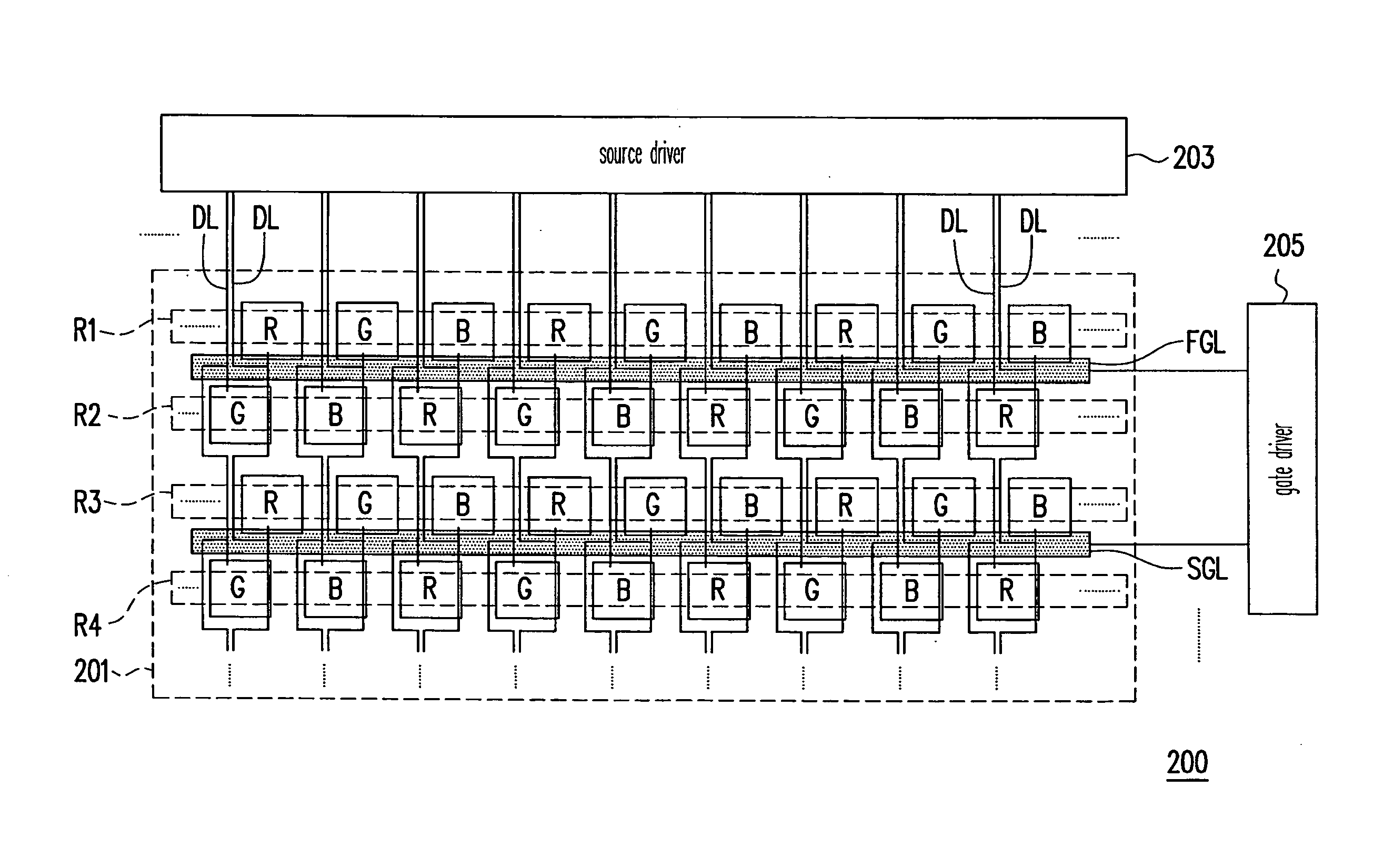
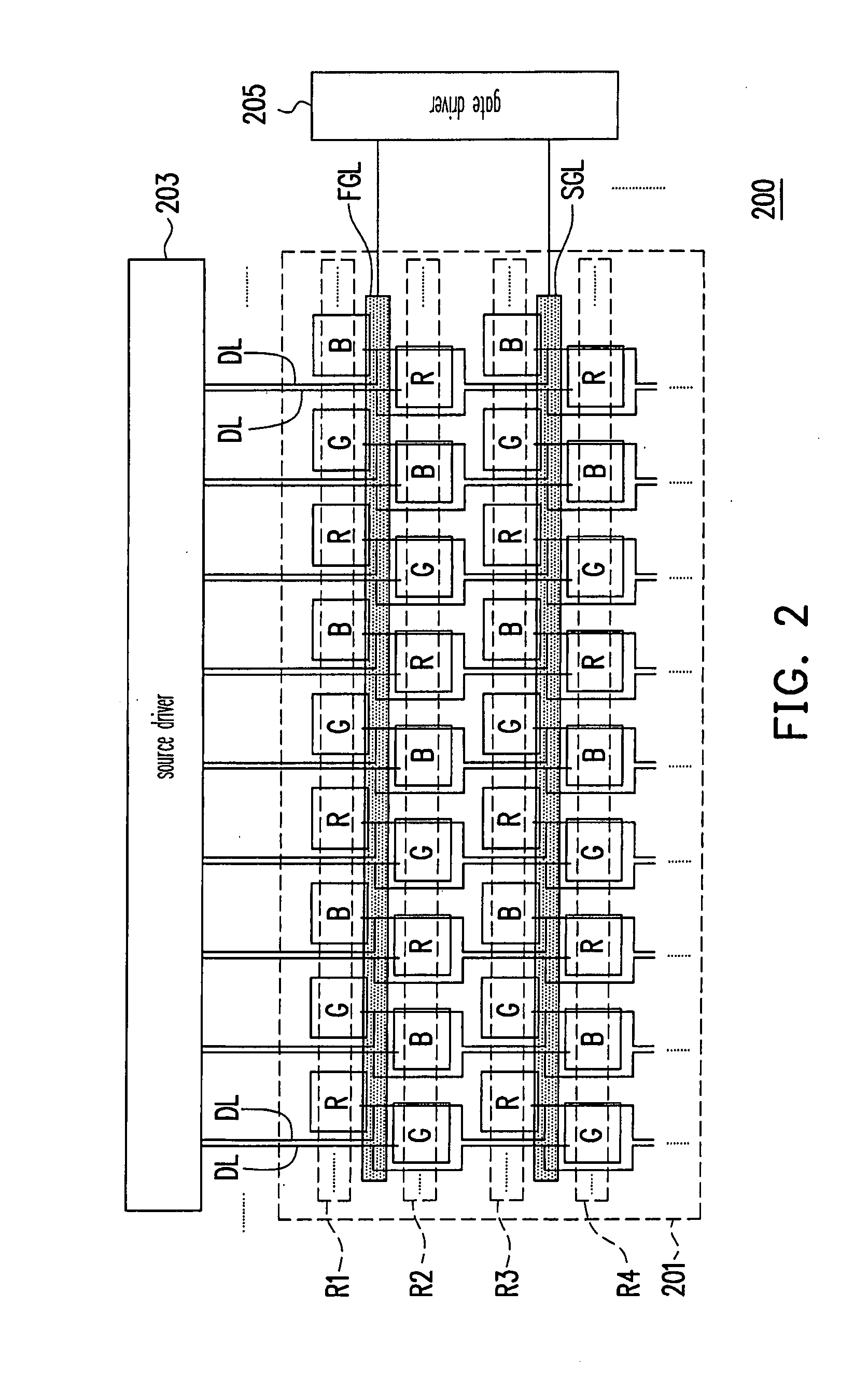
[0026]FIG. 2 illustrates a display according to a first embodiment of the invention. The display 200 may be any of known flat displays, such as an LCD or a plasma display panel (PDP). Referring to FIG. 2, the display 200 is taken as an LCD display for an example, wherein the display 200 includes a display panel 201, a source driver 203, and a gate driver 205. The display panel 201 includes a pixel array, a first scan line FGL, a second scan line SGL and a plurality of data lines DL disposed on a substrate (not shown). In the first embodiment, the first scan line FGL is electrically connected with the first sub-pixel row R1 and the second sub-pixel row R2, and second scan line SGL is electrically connected with the third sub-pixel row R3 and the fourth sub-pixel row R4. The sub-pixels in adjacent sub-pixel rows among the sub-pixel rows R1-R4 are staggered in order to form a delta type pixel array.

[0027]A plurality of data lines DL in the pixel array of the display...

second embodiment

The Second Embodiment

[0036]FIG. 4 illustrates a display 400 according to the second embodiment of the present invention. Referring to both FIGS. 2 and 4, the difference between the display 400 and the display 200 is that the wire arrangements of the first and the second groups of data lines DL in the display panel 401 in FIG. 4 differ from the wire arrangements of the data lines DL in the display panel 201 in FIG. 2.

[0037]In the second embodiment, each data line DL of the first group goes along the right side of each sub-pixel in the first sub-pixel row R1, circles leftward under the said sub-pixel in the first sub-pixel row R1 and electrically connects with the sub-pixel. Furthermore, the data line DL goes along the left side of a corresponding sub-pixel in the adjacent staggered second sub-pixel row R2 and circles rightward under the said sub-pixel. Then, the data line DL goes further along the right side of another corresponding sub-pixel in the adjacent staggered third sub-pixel...

third embodiment

The Third Embodiment

[0040]FIG. 6 illustrates a display 600 according to the third embodiment of the present invention. Referring to both FIGS. 2 and 6, the most significant difference between a display 600 and the display 200 is that the data lines DL of the pixel array in a display panel 601 of the display 600 are divided into six groups and that the wire arrangements of the data lines DL in the pixel array of the display panel 601 also differ from the wire arrangements of the data lines DL in the pixel array of the display panel 201. However, the desired effects and the technical problems to be solved of the display panel 600 are the same as those of the display 200.

[0041]In the third embodiment, each data line DL of the first group goes along the right side of a corresponding sub-pixel in the first sub-pixel row R1, circles leftward under the said sub-pixel in the first sub-pixel row R1 and electrically connects with the sub-pixel. Furthermore, the data line DL goes along the lef...


PUM


Abstract

A pixel array and a display panel with the pixel array are provided. The number of the scan lines used in the pixel array is reduced to half, while the number of data lines is doubled because every two sub-pixel rows correspond to one scan line in the pixel array. The wire impedances between the data lines and the pixel array are thus made the same. The aperture ratio of each sub-pixel is thereby increased and the size of the TFT in each sub-pixel is also reduced. The complexity in the wire arrangement of the pixel array is accordingly lowered to improve the transmittance of the display panel and make the frame resolution of the display panel more even.

Description

CROSS-REFERENCE TO RELATED APPLICATION[0001]This application claims the priority benefit of Taiwan application serial no. 95143159, filed on Nov. 22, 2006. All disclosure of the Taiwan application is incorporated herein by reference.BACKGROUND OF THE INVENTION[0002]1. Field of the Invention[0003]The present invention relates to a display panel, and especially to the pixel layout of a pixel array and a display panel applying the same.[0004]2. Description of Related Art[0005]FIG. 1 is a schematic diagram of a conventional liquid crystal display. The liquid crystal display 100 includes a display panel 101 having a delta type pixel array, a plurality of data lines DL, and a plurality of scan lines GL disposed thereon. Referring to FIG. 1, the sub-pixels of the first and the last sub-pixel rows are not disposed on the same shaft. Hence, the wire arrangement of the data lines in the display panel 101 is in a step-type arrangement. Each of the data lines DL in the display panel 101 is corr...

Claims


Application Information

Patent Timeline
IPC IPC(8): G09G3/36
CPCG09G3/3648G09G2300/0465G09G2300/0452G09G2300/0426
Inventor YEH, YIH-YUAN
Owner AU OPTRONICS CORP
Why Eureka
Try Eureka