Memory readout circuit and phase-change memory device

a memory readout and phase-change memory technology, applied in the field of phase-change memory, can solve problems such as difficult fast reading out, and achieve the effects of fast readout operation, preventing read disturb, and large set readout curren

Inactive Publication Date: 2008-05-22
LONGITUDE SEMICON S A R L
View PDF3 Cites 31 Cited by
  • Summary
  • Abstract
  • Description
  • Claims
  • Application Information

AI Technical Summary

Benefits of technology

[0053]The memory readout circuit of the present invention sets the readout voltage to higher, and reads out dynamic resistance at readout of a set state. Since the dynamic resistance is less than set resistance, a large set readout current is obtained. Thus, it is possible to obtain the effect to be capable of a fast readout operation. Further, the readout circuit includes a slowly cooling circuit. The slowly cooling circuit slowly cools the phase-change element after reading out data, thereby preventing read disturb. This makes it possible to restore the phase-change element to a set state. By constructing in this manner, a readout circuit and a system capable of fast readout, and a phase-change memory device provided with the readout circuit can be obtained.

Problems solved by technology

There has been a problem that a readout current at a set state becomes smaller, and this makes it difficult to read out fast.

Method used


Image

  • Memory readout circuit and phase-change memory device
  • Memory readout circuit and phase-change memory device
  • Memory readout circuit and phase-change memory device

Examples


first embodiment

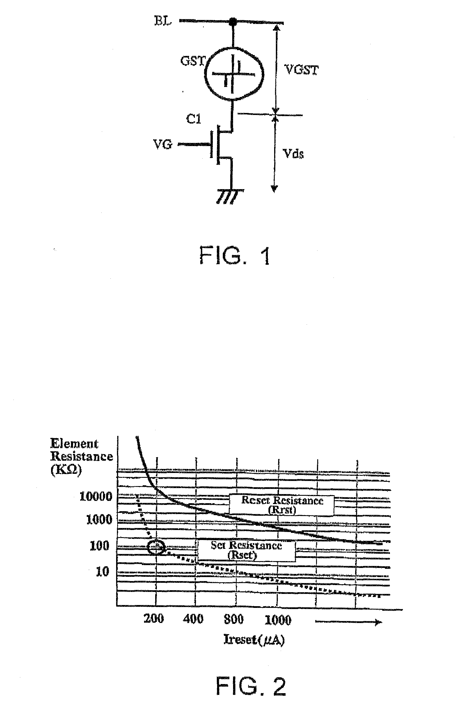
[0085]A readout circuit for a phase-change memory according to a first embodiment of the present invention will now be described in detail with reference to FIG. 9 and FIGS. 11 to 14. FIG. 9 is a circuit diagram of a readout circuit according to a first embodiment of the present invention. FIG. 11 and FIG. 12 respectively show a waveform diagram of operating voltage and a waveform diagram of an operating current, FIG. 13 and FIG. 14 respectively show volt-ampere characteristics of the phase-change element at reset and set states.

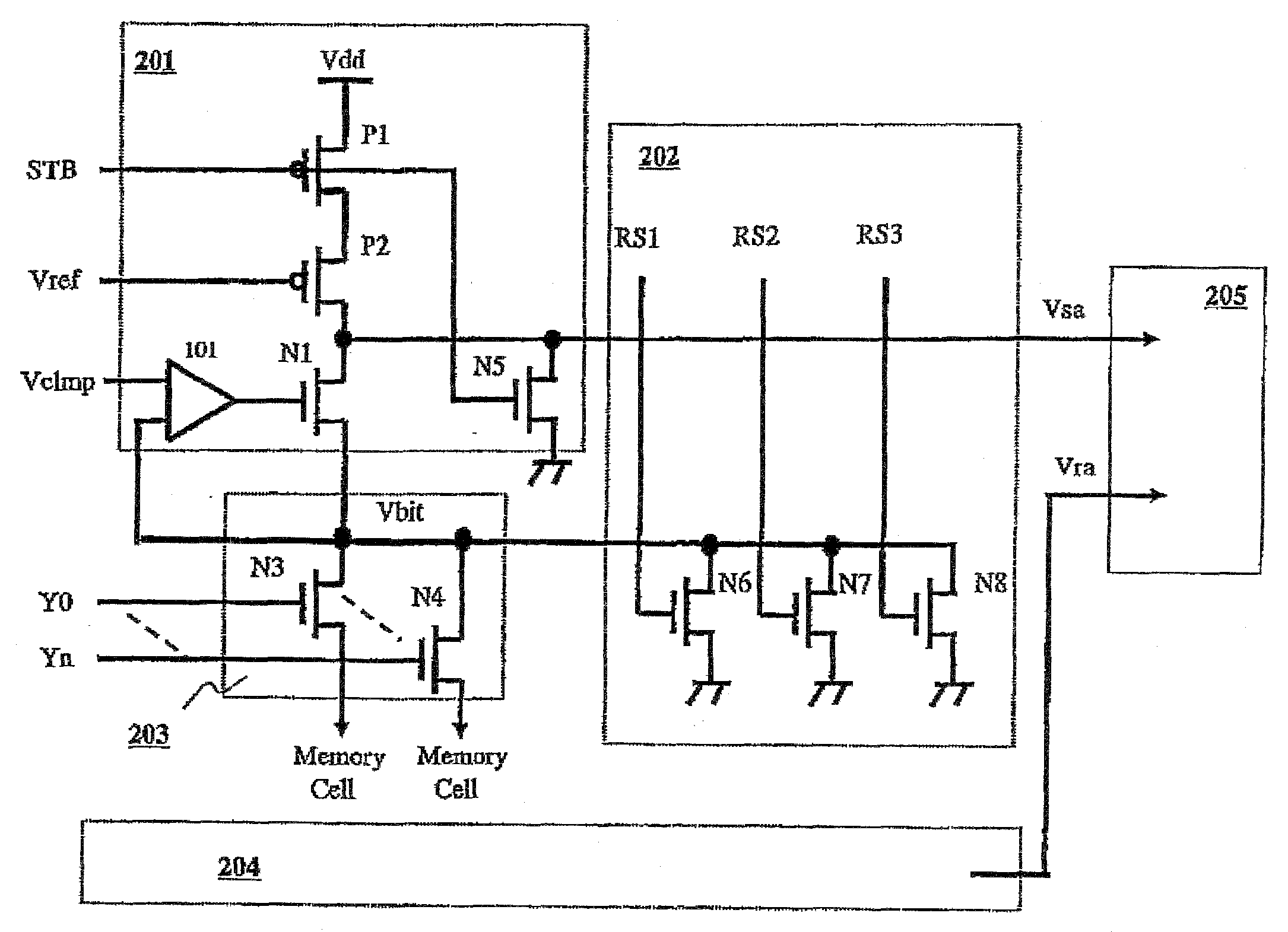
[0086]In FIG. 9, the readout circuit is constituted from a sense amplifier 201, a slowly cooling circuit 202, a Y switch 203, a reference amplifier 204 and a latch amplifier circuit 205. In readout, a bit line of a memory cell is first selected by the Y switch 203, and stored data are read out to the connection node Vbit. The stored data of the connection node Vbit are inputted to the sense amplifier 201, and the sense amplifier 201 outputs it as the sense a...

second embodiment

[0109]A readout circuit according to a second embodiment of the present invention will be described in detail with reference to FIGS. 15 to 17. The present embodiment is an embodiment providing a second circuit configuration of the readout circuit in which the slowly cooling circuit 202 in the readout circuit of the first embodiment is changed. FIG. 16 shows a block diagram of a second readout circuit. FIG. 16 and FIG. 17 respectively show waveform diagrams of operating voltage and current are respectively.

[0110]The readout circuit is constituted from a sense amplifier 201, a slowly cooling circuit 202, a Y switch 203, a reference amplifier 204, and a latch amplifier circuit 205. In this configuration, the sense amplifier 201, the Y switch 203, the reference amplifier 204, and the latch amplifier circuit 205 respectively have same configurations as those in the first embodiment. Parts of the same configuration will briefly be described.

[0111]The sense amplifier 201 is the same as th...

third embodiment

[0124]A readout circuit according to a third embodiment of the present invention will be described in detail with reference to FIG. 18. The present embodiment is an embodiment providing a third circuit configuration of the readout circuit in which the slowly cooling circuit 202 in the readout circuit is changed. FIG. 18 shows a block diagram of a third readout circuit.

[0125]The readout circuit is constituted from a sense amplifier 201, a slowly cooling circuit 202, a Y switch 203, a reference amplifier 204, and a latch amplifier circuit 205. In this configuration, the sense amplifier 201, the Y switch 203, the reference amplifier 204, and the latch amplifier circuit 205 respectively have same configurations as those in the first embodiment. Parts of the same configuration will briefly be described.

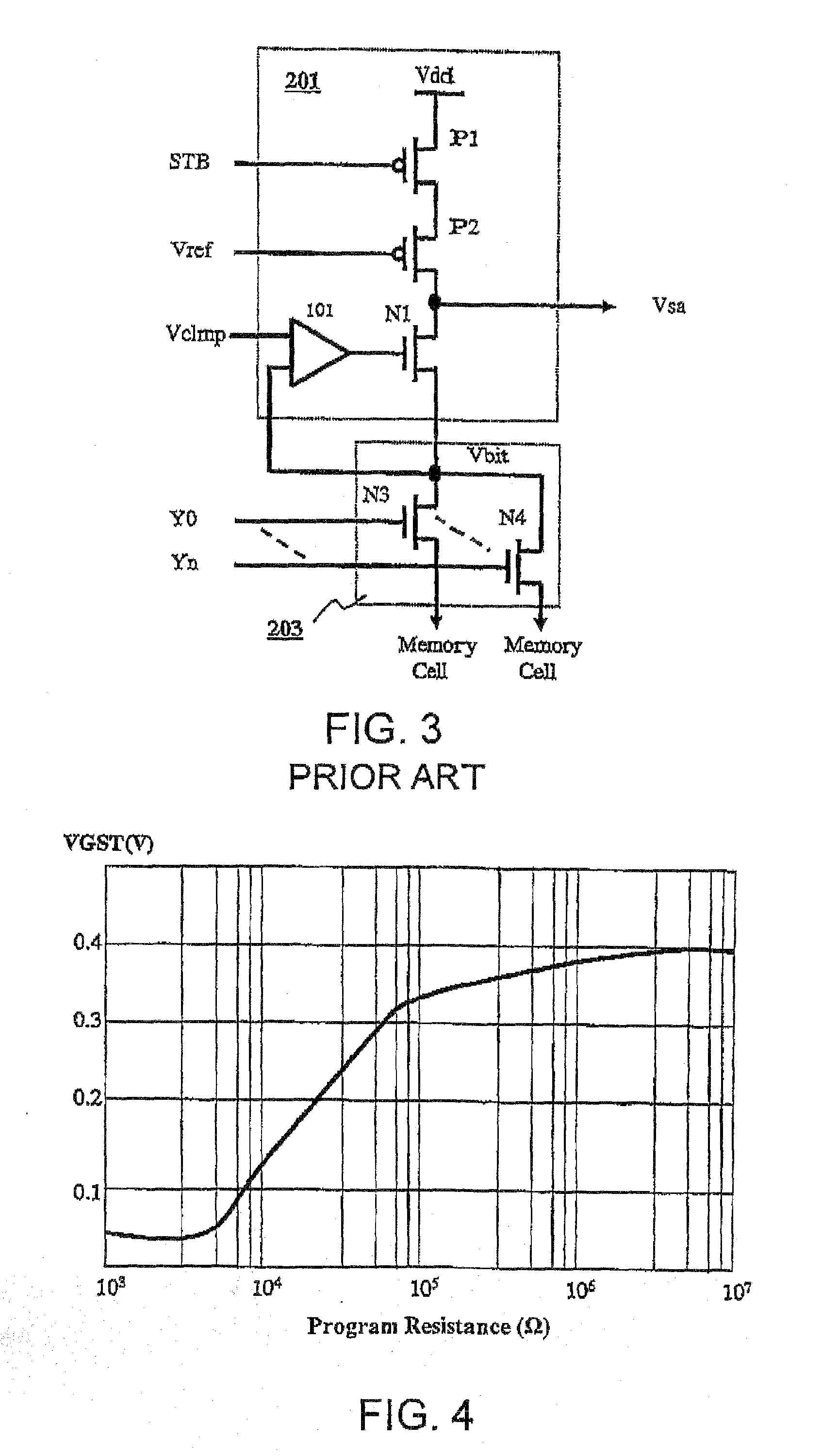
[0126]The sense amplifier 201 is the same as the circuit shown in FIG. 9. The sense amplifier 201 is constituted from transistors P1, P2, N1, and N5, and a comparator circuit 101. The tran...


PUM


Abstract

In a memory readout circuit for use in a phase-change memory device comprising phase-change elements as memory cells, a sense amplifier sets readout voltage, which is applied to a selected phase-change element selected among the phase-change elements by a column selecting switch, to voltage equal to or higher than hold voltage of the selected phase-change element but lower than transition voltage of the selected phase-change element in a readout cycle. The selected phase-change element is read out as a dynamic state in the case where the selected phase-change element is in a set state.

Description

[0001]This application is based upon and claims the benefit of priority from Japanese patent application No. 2006-314215, filed on Nov. 21, 2006, the disclosure of which is incorporated herein in its entirety by reference.BACKGROUND OF THE INVENTION[0002]The present invention relates to a phase-change memory and, in particular, to a readout circuit for use in the phase-change memory.[0003]A semiconductor memory includes a volatile memory which loses memory information when power supply is turned off and a nonvolatile memory which retains memory information even when power supply is turned off. For example, the volatile memory is a Dynamic Random Access Memory (DRAM) or a Static Random Access Memory (SRAM), while the nonvolatile memory is an Electrically Erasable Programmable Read Only Memory (EEPROM) or a flash memory. In a recent mobile information terminal, for the purpose of miniaturization and power saving, the flash memory which retains memory information even when power supply...

Claims


Application Information

Patent Timeline
Patent Type & Authority Applications(United States)
IPC IPC(8): G11C11/00
CPCG11C13/0004G11C13/004G11C2013/0092G11C2013/0052G11C2013/0054G11C13/0069
Inventor FUJI, YUKIOTONOMURA, YASUKO
Owner LONGITUDE SEMICON S A R L
Why Eureka
Try Eureka