Monocrystalline extrinsic base and emitter heterojunction bipolar transistor and related methods

a monocrystalline extrinsic base and emitter technology, applied in the field of integrated circuit (ic) chip fabrication, can solve the problems of polycrystalline extrinsic base, performance degradation, and inability to achieve the effect of hbt,

Inactive Publication Date: 2008-05-29
IBM CORP
View PDF4 Cites 21 Cited by
  • Summary
  • Abstract
  • Description
  • Claims
  • Application Information

AI Technical Summary

Benefits of technology

[0005]A heterostructure bipolar transistor (HBT) and related methods are disclosed. In one embodiment, the HBT includes a heterostructure bipolar transistor (HBT) comprising: a substrate; a monocrystalline emitter atop the substrate; a collector in the substrate; at least one isolation region adjacent to the collector; a monocrystalline silicon germanium (SiGe) intrinsic base extending over each i

Problems solved by technology

Advancement of SiGe HBT technology, however, is hindered by a number of challenges.
Even small misalignments and device size increases result in performance degradation due to increased overlap capacitances, even device failure.
These known approaches result in problems such as emitter and base mis-alignment and non-planarity, a disc

Method used


Image

  • Monocrystalline extrinsic base and emitter heterojunction bipolar transistor and related methods
  • Monocrystalline extrinsic base and emitter heterojunction bipolar transistor and related methods
  • Monocrystalline extrinsic base and emitter heterojunction bipolar transistor and related methods

Examples


Embodiment Construction

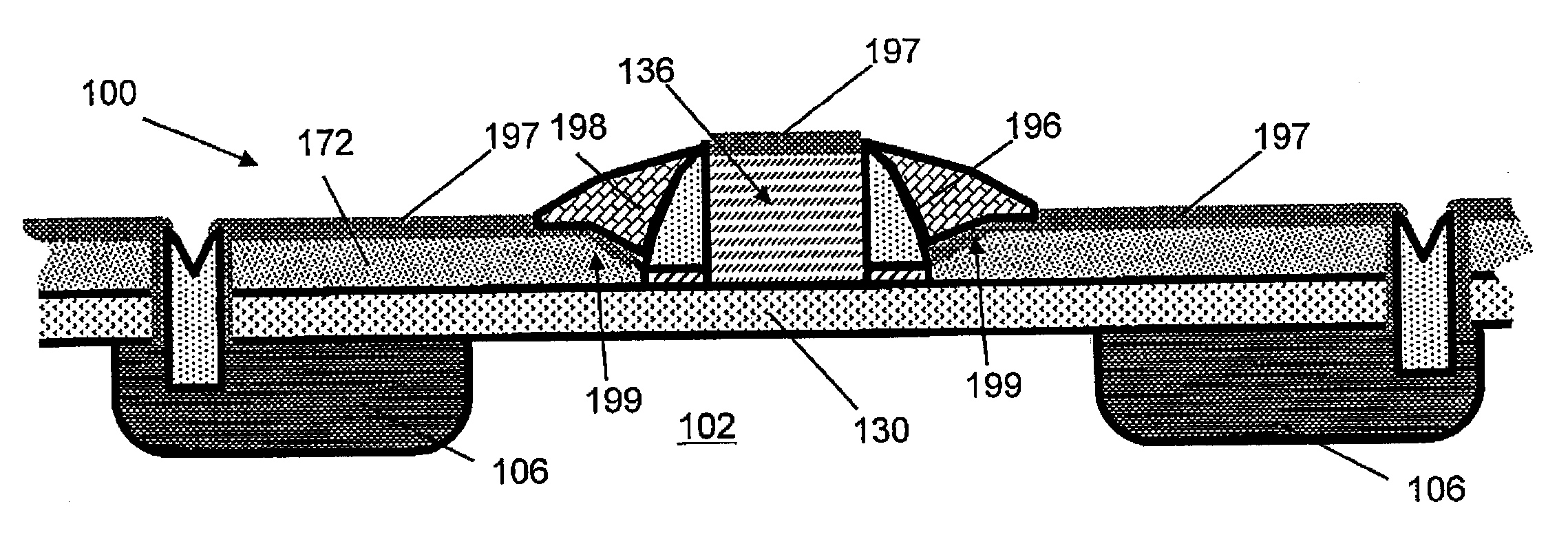
[0018]Turning to the drawings, FIGS. 1-29 show various embodiments of a method, and in particular, a method of forming a heterostructure bipolar transistor (HBT) 100, 200 (FIGS. 17, 25 and 27-29).

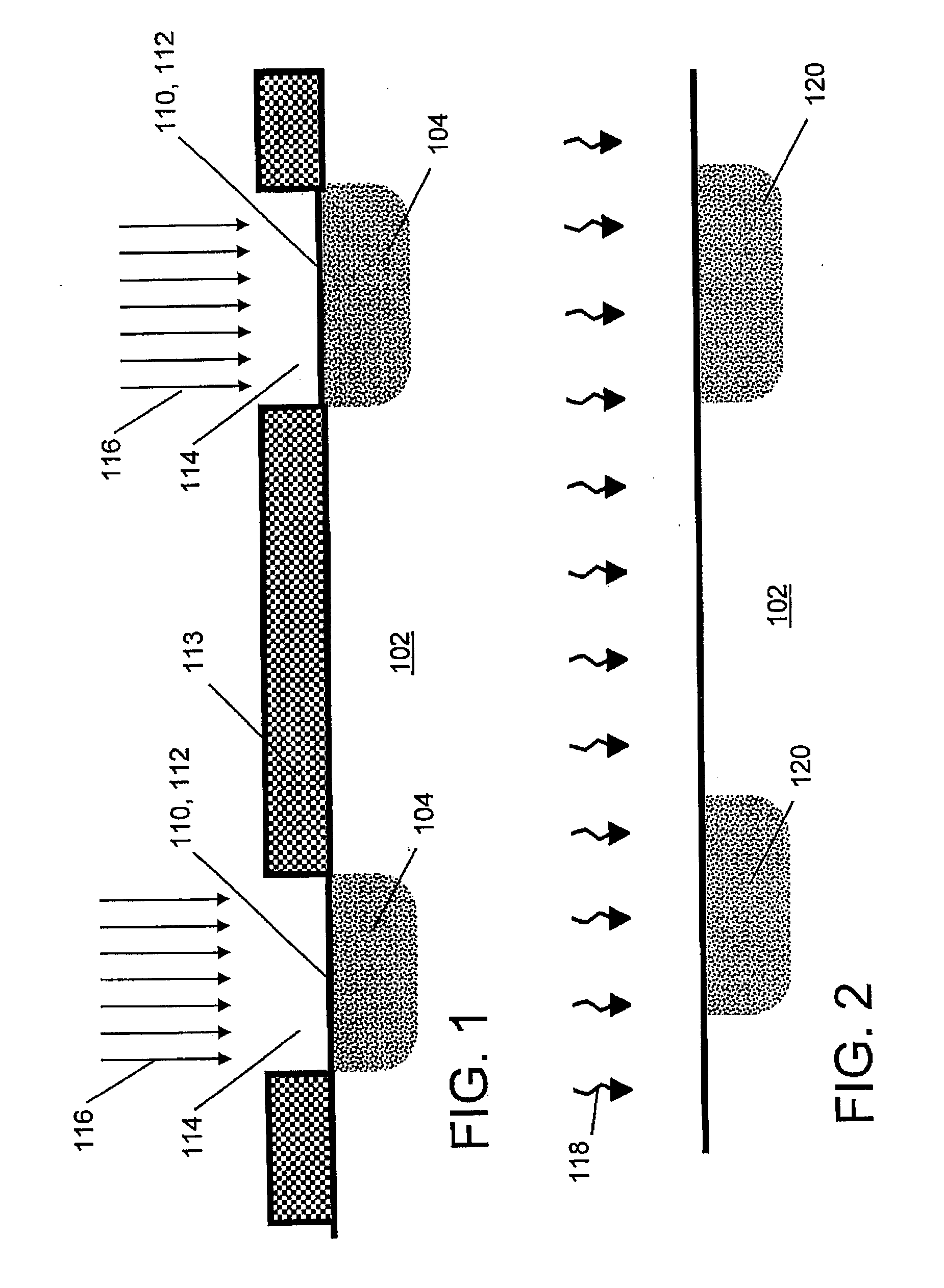
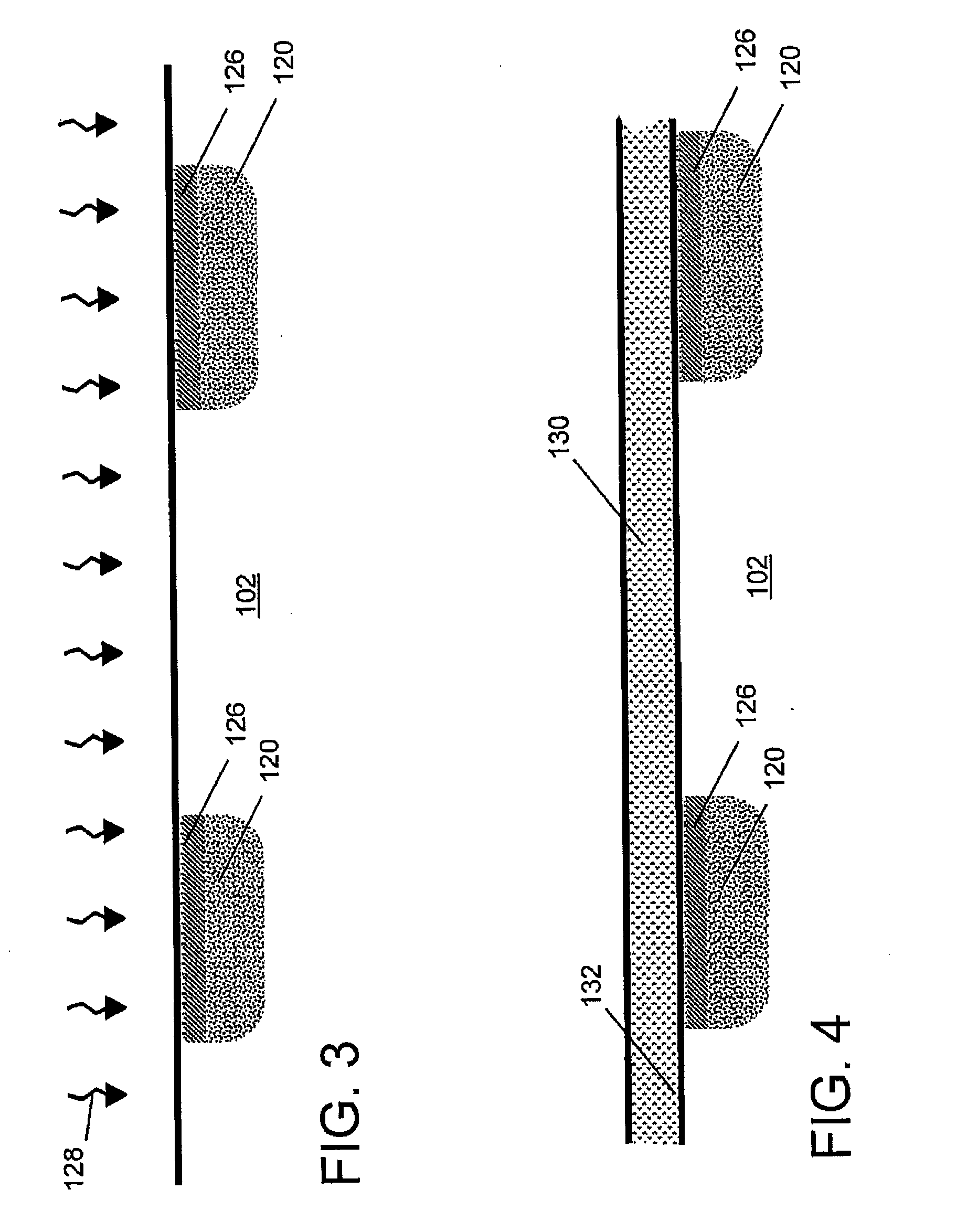
[0019]FIGS. 1-17 show one embodiment of the method. FIG. 1 shows providing a substrate 102. Substrate 102 may include but is not limited to: silicon or silicon germanium, in the form of a bulk, semiconductor-on-insulator (SOI), or virtual substrate (relaxed SiGe). In any case, substrate 102 is monocrystalline. FIG. 1 also shows one embodiment of forming an implanted region 104 (two shown) in substrate 102, which will ultimately become isolation region 106 (FIG. 13), as described herein. Implanted region 104 includes an upper surface 110 capable of having monocrystalline silicon formed thereon. In this case, implanted region 104 includes the monocrystalline silicon (now doped) of substrate 102. Implanted region 104 may be formed, for example, by forming a mask 113 and patterning / etching to f...


PUM


Abstract

A heterostructure bipolar transistor (HBT) and related methods are disclosed. In one embodiment, the HBT includes a heterostructure bipolar transistor (HBT) including: a substrate; a monocrystalline emitter atop the substrate; a collector in the substrate; at least one isolation region adjacent to the collector; a monocrystalline silicon germanium (SiGe) intrinsic base extending over each isolation region; and a monocrystalline silicon extrinsic base. A method may include forming the intrinsic and extrinsic base and the emitter as monocrystalline, with the extrinsic base (and emitter) formed in a self-aligned fashion utilizing selective-epitaxial growth on porous silicon. As a result, some mask levels can be omitted, making this an inexpensive alternative to conventional processing.

Description

BACKGROUND OF THE INVENTION[0001]1. Technical Field[0002]The invention relates generally to integrated circuit (IC) chip fabrication, and more particularly, to a heterojunction bipolar transistor (HBT) with a monocrystalline base and emitter and methods related thereto.[0003]2. Background Art[0004]Silicon germanium (SiGe) heterostructure bipolar transistors (HBT) are high performance transistor structures used widely in high-speed integrated circuit (IC) chips. Advancement of SiGe HBT technology, however, is hindered by a number of challenges. For example, to meet costumer demands and market trends toward higher speeds and lower power consumption, devices are scaled, i.e. reduced in size. Consequently, small lithographic printing dimensions and the ability to align mask levels with extreme precision are required. Even small misalignments and device size increases result in performance degradation due to increased overlap capacitances, even device failure. In addition, current high-p...

Claims


Application Information

Patent Timeline
IPC IPC(8): H01L29/737H01L21/331
CPCH01L29/0821H01L29/7378H01L29/66242
Inventor ADAM, THOMAS N.WALLNER, THOMAS A.
Owner IBM CORP
Why Eureka
Try Eureka