Semiconductor device

a technology of semiconductor devices and devices, applied in the direction of semiconductor devices, electrical devices, transistors, etc., can solve the problems of machining shape of gates, inhibiting the improvement of high frequency, and unnecessary gate capacities cgd and cgs, and achieves small variation in gate width and favorable matching characteristics.

Active Publication Date: 2008-05-29
PANASONIC SEMICON SOLUTIONS CO LTD
View PDF6 Cites 8 Cited by
  • Summary
  • Abstract
  • Description
  • Claims
  • Application Information

AI Technical Summary

Benefits of technology

[0034]It is a first object of the present invention to eliminate unnecessary gate capacity addition and to improve high frequency characteristics including noise, the maximum oscillation frequency, and the like in a semiconductor device, such as a MOSFET or the like, having unit cells with ring-shaped gate electrodes arranged in an array.
[0035]Further, it is a second object of the present invention to, in addition to achieving the first object described above, reduce characteristic variation even when a machining shape of a bending portion of the gate electrode is unstable.
[0060]In particular, in the present invention, bending portions of the gate electrode, where a machining shape is unstable, lie outside of the active region not directly related to transistor operation, thus permitting formation of a MOSFET with small variation in the gate width. Further, for example, employing a square shape for the ring-shaped gate electrode in the unit cell secures a configuration with a stable four-way gate, thus forming anywhere on the semiconductor substrate a unit cell averagely undergoing a two-way process fluctuation (e.g., in formation of the source region and the drain region, an ion implantation process for threshold control, gate machining dimension gradient). Thus, variation characteristics are uniform among a large number of unit cells and their characteristics almost match with each other, thus permitting formation of a MOSFET with a favorable matching characteristic.

Problems solved by technology

Consequently, unnecessary gate capacities Cgd and Cgs are added, which presents the drawback of inhibiting an improvement in the high frequency characteristics, such as noise and the maximum oscillation frequency in particular, as indicated in the formulae (4) and (5) provided for “performance requirements imposed on the high-frequency silicon MOSFET” described above.
The presence of a portion of the gate drawing wire 5 not drawn out, if any, results in the presence of a region where the gate electrode 1 is bent and a machining shape of the gate at this portion becomes unstable, thus presenting the drawback that a MOSFET with little characteristic variation cannot be provided.
On the other hand, patent documents 2 and 3 do not at all disclose that gate contact regions and gate drawing wires are provided on an individual unit transistor basis.

Method used


Image

  • Semiconductor device
  • Semiconductor device
  • Semiconductor device

Examples


first embodiment

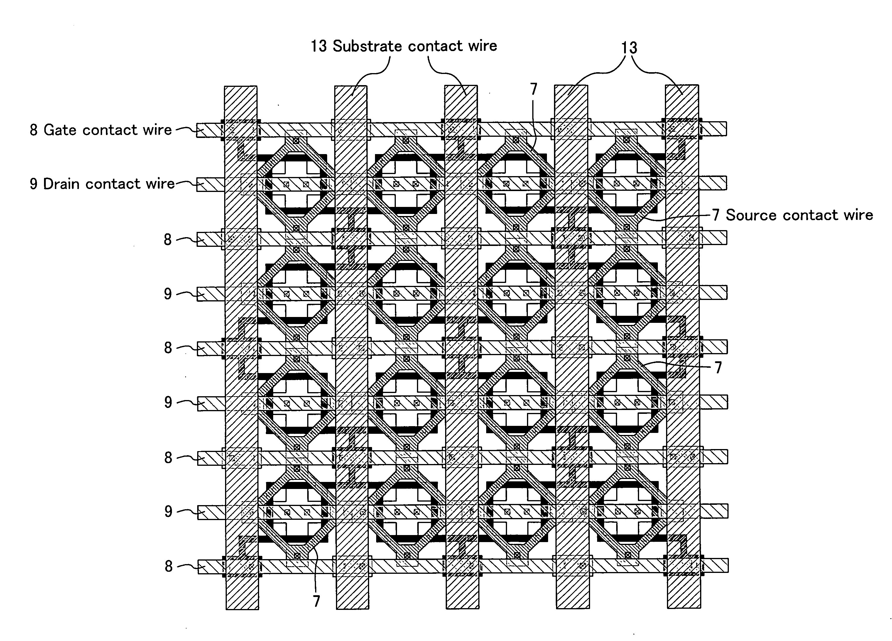
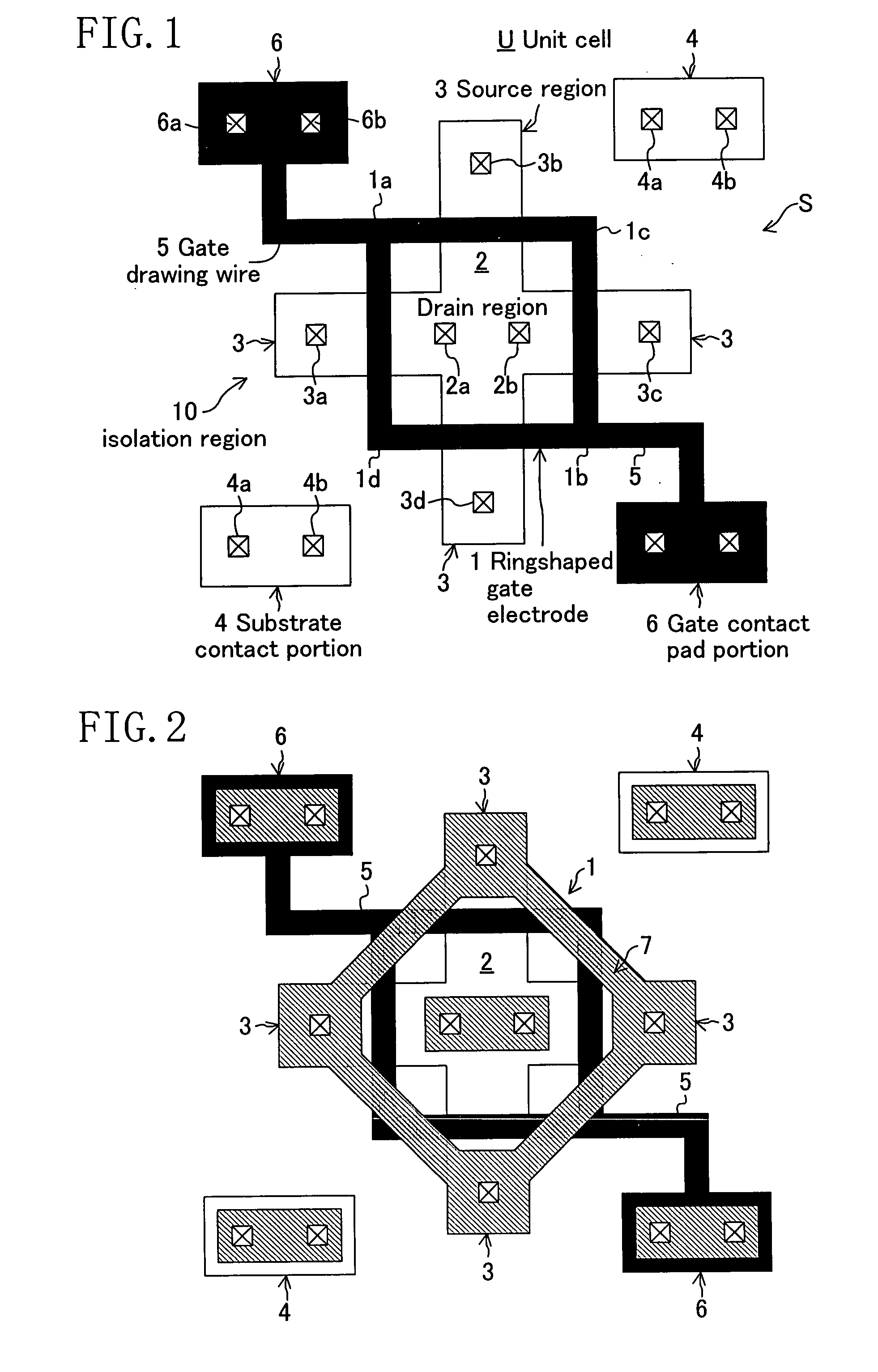
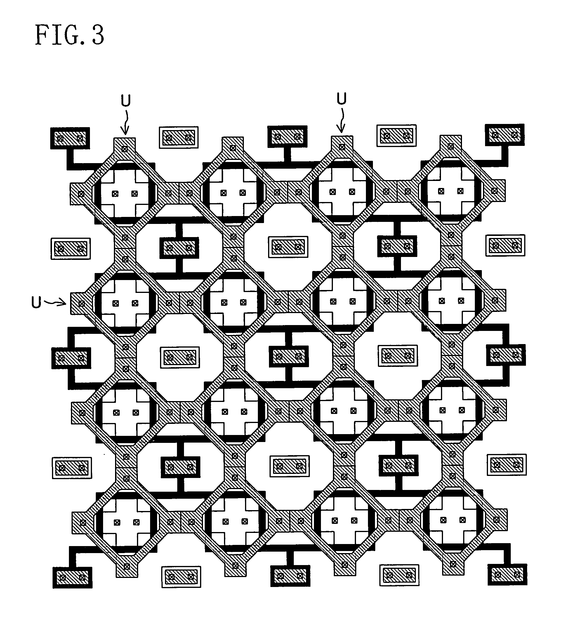
[0083]FIG. 1 is a plan view schematically showing a layout configuration of a unit cell of a MOSFET as a semiconductor device according to the first embodiment of the present invention. FIG. 2 is a diagram showing the unit cell of FIG. 1 with a first layer wire added thereto. FIG. 3 is a plan view showing a cell array structure of the entire MOSFET referring to the unit cell structure shown in FIG. 2 as an example, and such a MOSFET functions as, for example, a high-frequency signal amplification FET. A large number of unit cells are formed and arranged laterally and longitudinally in an orderly manner in FIG. 3, and only one of these unit cells is shown in FIG. 1.

[0084]In the unit cell U of FIG. 1, on a semiconductor substrate S of silicon, a transistor is formed with a cross-shaped active region being formed in a region surrounded by an isolation region 10 of a separating insulating film and with the center of this active region being surrounded by a square ring-shaped gate electr...

second embodiment

[0097]FIG. 7 is a plan view schematically showing a layout of a unit cell U of a MOSFET according to the second embodiment of the present invention. FIG. 8 is a diagram of FIG. 7 with a first layer wire added thereto. FIG. 7 is a plan view illustrating the structure of the unit cell U according to the present embodiment, for the purpose of showing the cell array structure of the MOSFET according to the present embodiment.

[0098]This structure locates the gate electrode 1 in FIG. 1 at such a position that diminishes the gate drawing wires 5 to the minimum. In the unit cell U shown in FIG. 7, a drain region 2 has an area set small such that only one drain contact 2a can be formed thereon, and four source regions 3 each have one source contact 3a formed thereon, so that four source contacts 3a are provided per unit cell U. Two gate contact pad portions 6 each have an area set small such that only one gate contact 6a can be provided thereon. FIG. 7 shows the layout of the unit cell U ach...


PUM


Abstract

In a semiconductor device, such as a MOSFET or the like, which is a high-frequency LSI achieving a low noise figure and a high maximum oscillation frequency and which has unit cells with a ring-shaped gate electrode arranged in an array, gate drawing wires connecting together the gate electrode and gate contact pad portions are arranged on a region excluding a drain region and a source region, that is, on an isolation region. Bending portions of the ring-shaped gate electrode are all formed on the isolation region. This therefore permits an improvement in high frequency characteristics such as noise, the maximum oscillation frequency, and the like while eliminating unnecessary gate capacity addition, and also permits small characteristic variation even if a machining shape of the bending portions of the gate electrode is unstable.

Description

CROSS REFERENCE TO RELATED APPLICATIONS[0001]This non-provisional application claims priority under 35 U.S.C. §119(a) on Patent Application No. 2006-168935 filed in Japan on Jun. 19, 2006, the entire contents of which are hereby incorporated by reference.BACKGROUND OF THE INVENTION[0002]1. Technical Field[0003]The present invention relates to a device structure of a MOSFET having excellent high-frequency characteristics.[0004]2. Related Art[0005]In recent years, the mobile communication market has been expanding due to increasing demand, system sophistication, and widened applicability of mobile communication technology, and it is estimated that the market size of mobile communication services and appliances can reach 11 trillion yen in 2010. Accordingly, great expectation is put on transistors and ICs capable of handling frequency bands in the GHz region, which is suitable for use in communication appliances, mobile radio base stations, satellite communication, broadcast stations, ...

Claims


Application Information

Patent Timeline
Patent Type & Authority Applications(United States)
IPC IPC(8): H01L29/78
CPCH01L29/78H01L29/4238
Inventor SHIMOMURA, HIROSHI
Owner PANASONIC SEMICON SOLUTIONS CO LTD
Why Eureka
Try Eureka