Method and system for reducing the variation in film thickness on a plurality of semiconductor wafers having multiple deposition paths in a semiconductor manufacturing process

Inactive Publication Date: 2008-05-29
IBM CORP
View PDF13 Cites 11 Cited by
  • Summary
  • Abstract
  • Description
  • Claims
  • Application Information

AI Technical Summary

Benefits of technology

[0016]According to the present invention, there is disclosed a method for reducing the variation in film thickness on a plurality of semiconductor wafers having multiple deposition paths in a semiconductor manufacturing process. The method comprises the following steps: applying a film of a varying input thickness to the plurality of semiconductor wafers moving through a plurality of film deposition paths; recording the deposition path of each of the plurality of semiconductor wafers; measuring the input thickness of the film on selected semiconductor w

Problems solved by technology

Normal variations in temperature and reactant flow rate may cause a deviation in the deposition rate from the anticipated rate, causing the process to exceed a control limit.
The above method does not yield optimal results.
There is a desire to minimize the number of wafers sampled because measurement is considered to be a manufacturing overhead, and causes decreased manufacturing throughput.
However, some measurement is necessary because there can be considerable

Method used


Image

  • Method and system for reducing the variation in film thickness on a plurality of semiconductor wafers having multiple deposition paths in a semiconductor manufacturing process
  • Method and system for reducing the variation in film thickness on a plurality of semiconductor wafers having multiple deposition paths in a semiconductor manufacturing process
  • Method and system for reducing the variation in film thickness on a plurality of semiconductor wafers having multiple deposition paths in a semiconductor manufacturing process

Examples


Example

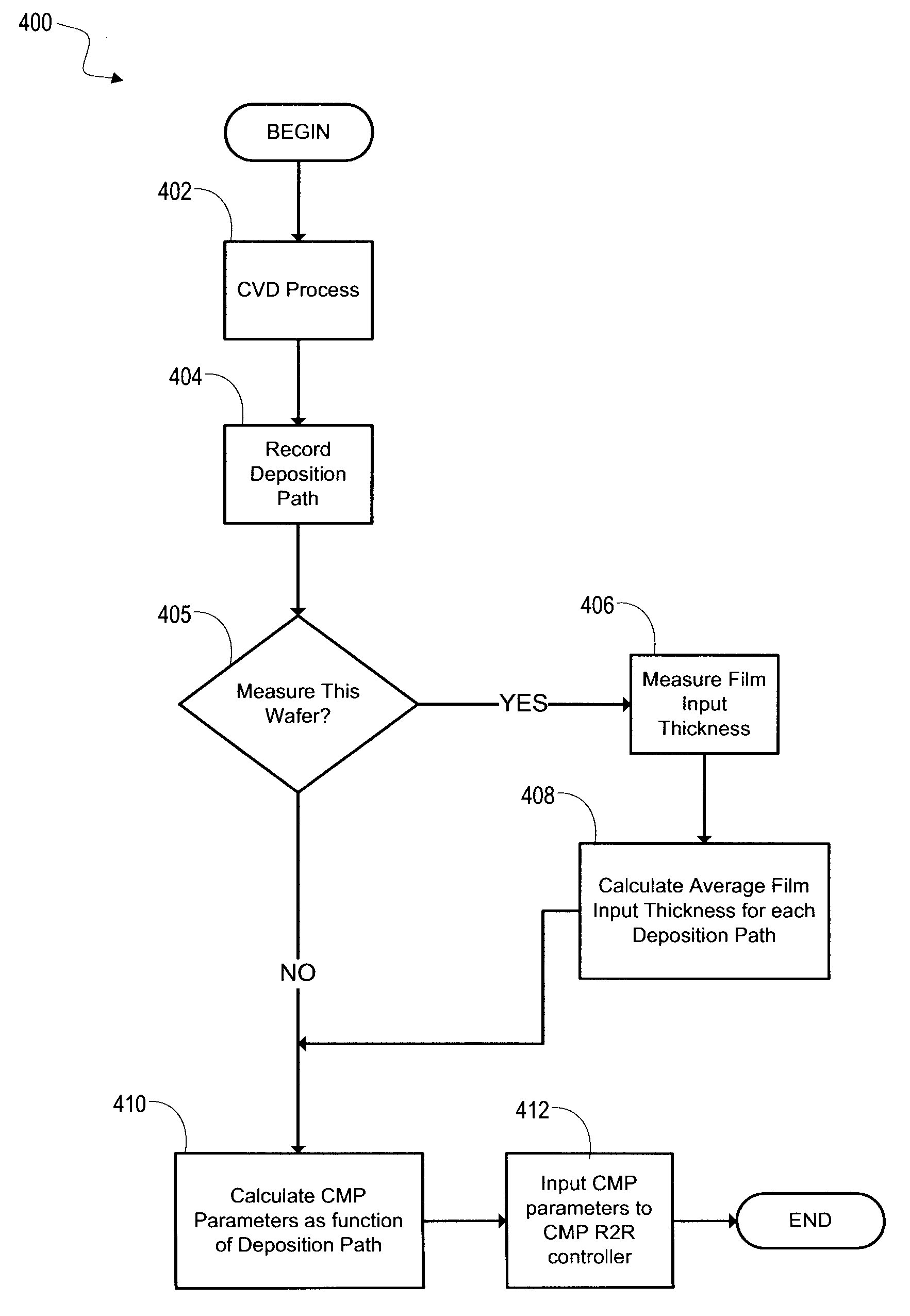
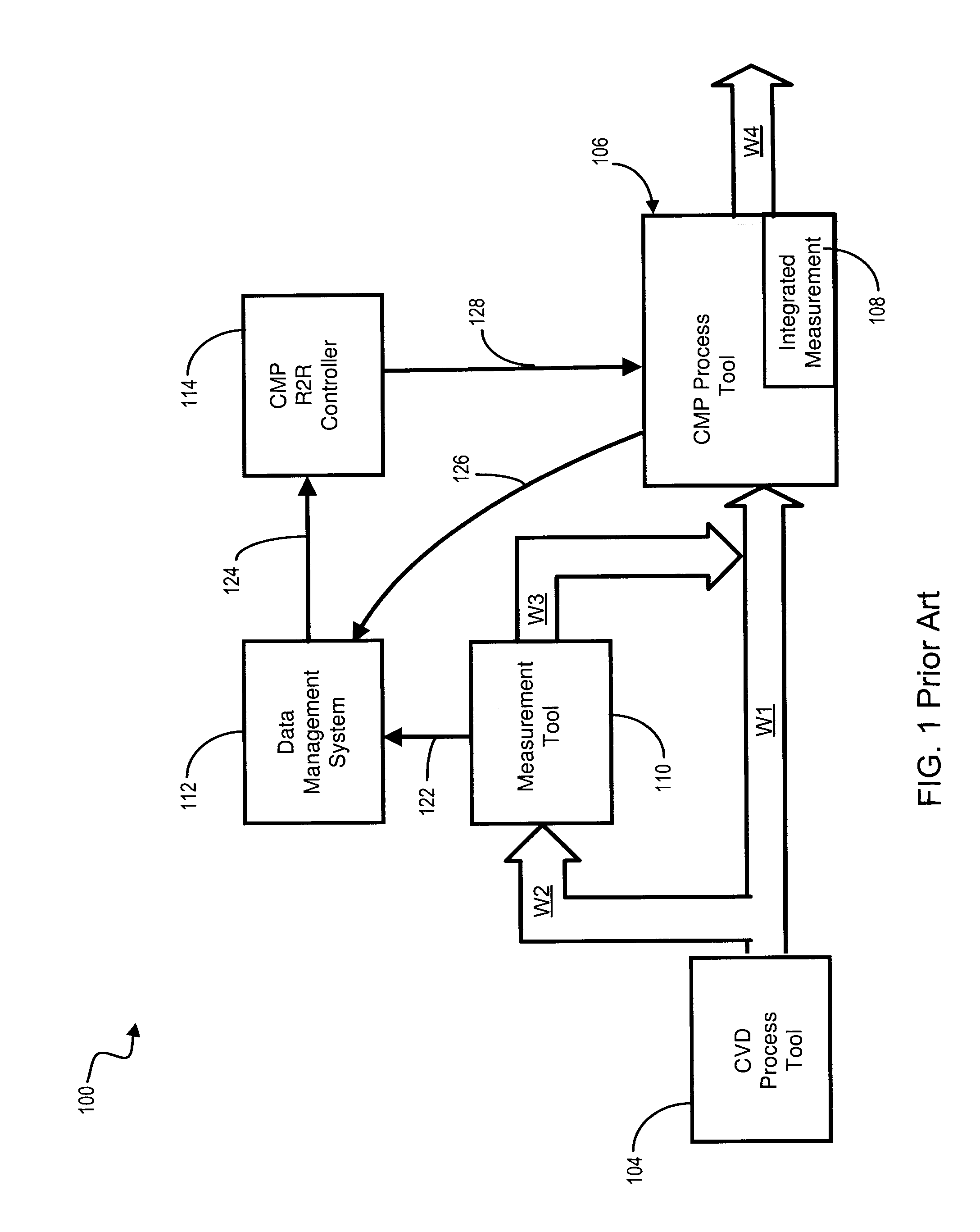
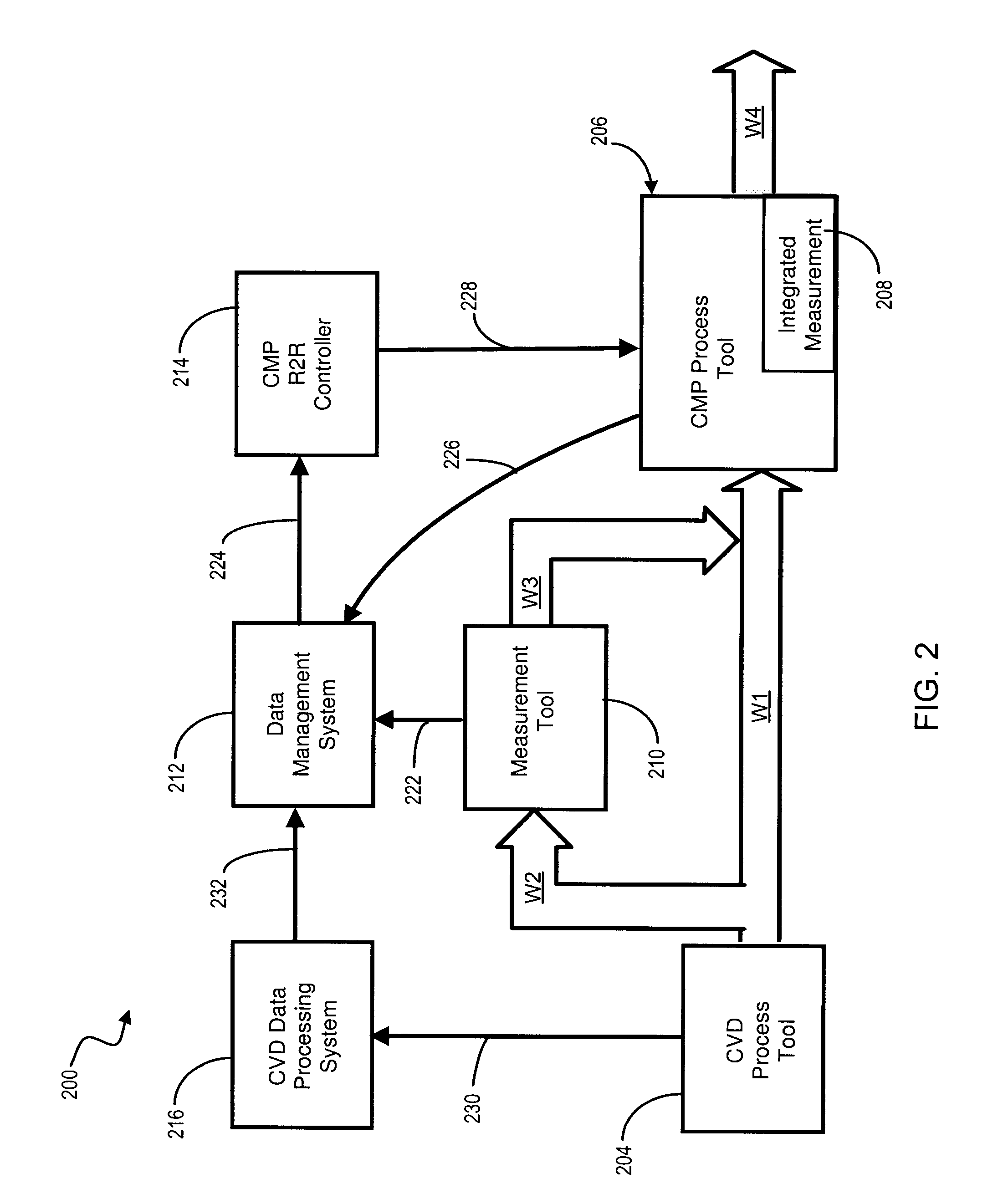
[0044]With reference to the accompanying drawings, FIG. 2 shows a block diagram of the system 200 the present invention. The system 200 encompasses all of the elements of prior art system 100 of FIG. 1, with the addition of a CVD Data Processing System 216, and associated data communication links 230 and 232. The CVD Data Processing System 216 records the specific CVD Process Tool and chamber within that tool from which a particular semiconductor wafer originated. This information is sent to the CVD Data Processing System 216 from the CVD Process Tool 204 via data communication link 230. This will be shown in more detail in FIG. 3. The specific tool and chamber used to perform CVD on a given semiconductor wafer is referred to as a “deposition path.” The CVD Data Processing System 216 provides deposition path specific data to the Data Management System 212 via data communication link 232. This data includes the deposition path specific data for each semiconductor wafer as it exits th...


PUM


Abstract

A method and system for reducing the variation in film thickness on a plurality of semiconductor wafers having multiple deposition paths in a semiconductor manufacturing process is disclosed. A film of a varying input thickness is applied to semiconductor wafers moving through various film deposition paths. The deposition path of each of the semiconductor wafers is recorded. A subset of semiconductor wafers is measured and an average film input thickness corresponding to each of the film deposition paths is calculated. If semiconductor wafer in the specific film deposition path does not have measurement data, by default it uses historical measurement data. The average film input thickness of the deposition path corresponding to a given semiconductor wafer is then used to modify the recipe of a process tool, such as a Chemical Mechanical Planarization (CMP) Process Tool. An improved manufacturing process is achieved without the use of excess measurements.

Description

FIELD OF THE INVENTION[0001]The present invention relates generally to semiconductor manufacturing, and, more particularly, to a method and apparatus for consistently making a film of a desired thickness on a semiconductor wafer in a manufacturing process flow.BACKGROUND[0002]In the manufacture of semiconductor devices, semiconductor wafers, such as silicon semiconductor wafers, are subjected to a number of processing steps. One such process step includes the depositing or forming of layers on the silicon semiconductor wafer. One such process used to form the layers is known as chemical vapor deposition (CVD), wherein reactive gases are introduced into a chamber, e.g., a CVD process tool, containing the semiconductor wafers. The reactive gases facilitate a chemical reaction that causes a layer to form on the semiconductor wafers. One exemplary deposition process is the formation of polysilicon by reacting nitrogen (N.sub.2) and silane (SiH.sub.4) in a furnace. Various types of CVD p...

Claims


Application Information

Patent Timeline
IPC IPC(8): H01L21/66B05C11/00
CPCH01L22/12
Inventor LI, YUEBEHM, GARY W.IANNUCCI, JAMES V.STOLL, DEREK C.
Owner IBM CORP
Why Eureka
Try Eureka