Method for manufacturing semiconductor device

a manufacturing method and semiconductor technology, applied in the direction of semiconductor devices, basic electric elements, electrical appliances, etc., can solve the problems of ineffective annealing, insufficient hydrogen termination of gate insulation films b>4/b>, and dangling bonds in the interface between silicon substrates

Inactive Publication Date: 2008-05-29
SANYO ELECTRIC CO LTD
View PDF0 Cites 13 Cited by
  • Summary
  • Abstract
  • Description
  • Claims
  • Application Information

AI Technical Summary

Benefits of technology

[0009]The present invention provides a manufacturing method in which annealing is effectively performed during the manufacture of a semiconductor device that uses tungsten as the contact material.

Problems solved by technology

Therefore, in the conventional tungsten plug structure, the Ti film 12 or the Ti deposited in the TiN film 14 without being nitrided during formation of the TiN traps hydrogen that is in the atmosphere or that diffuses from the deposited film to the interface between the silicon substrate 2 and the gate insulation film 4, and drawbacks occur in that the dangling bonds in the interface between the silicon substrate 2 and the gate insulation film 4 are not adequately terminated by hydrogen.
The annealing is therefore ineffective, and there are adverse effects on the device performance in a semiconductor device that handles charges generated by light or the like, such as a CCD image sensor or CMOS image sensor.
In a CCD image sensor, for example, the effects of titanium on the wiring portion that lines the transfer electrodes of the imaging portion can cause defects whereby dark currents increase in a photoreceptor pixel or a transfer portion.

Method used


Image

  • Method for manufacturing semiconductor device
  • Method for manufacturing semiconductor device
  • Method for manufacturing semiconductor device

Examples


Embodiment Construction

[0018]Embodiments of the present invention will be described hereinafter based on the drawings.

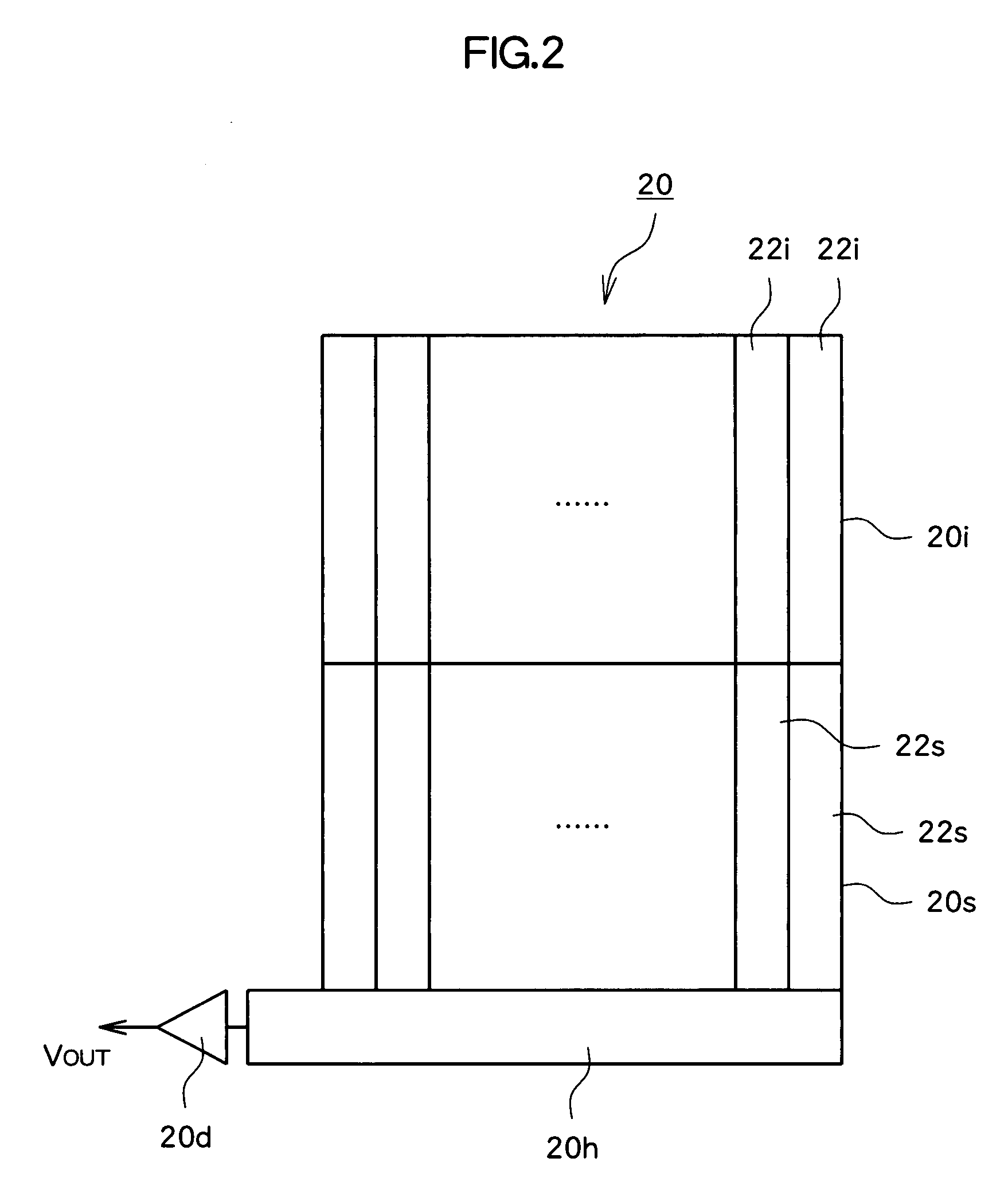
[0019]FIG. 2 is a schematic plan view showing the overall structure of a CCD image sensor as an embodiment of the present invention. FIG. 3 is a schematic plan view showing the overall arrangement of the polysilicon layers and the contacts in the CCD image sensor as an embodiment of the present invention.

[0020]The CCD image sensor 20 has a frame transfer architecture, and is provided with an imaging portion 20i, a storage portion 20s, a horizontal transfer portion 20h, and an output portion 20d formed on the surface of a semiconductor substrate.

[0021]The imaging portion 20i is composed of a plurality of vertical shift registers (vertical CCD shift registers) 22i arranged in the row direction (horizontal direction). The storage portion 20s is composed of a plurality of vertical shift registers 22s that correspond one-to-one to the plurality of vertical shift registers 22i of the imaging por...


PUM

PropertyMeasurementUnit
interface level densityaaaaaaaaaa
resistanceaaaaaaaaaa
charge transferaaaaaaaaaa

Abstract

An insulation film having an open part in which a silicon part is exposed at a bottom surface is formed on a silicon substrate for forming a semiconductor device. Titanium is deposited to form a titanium film on the bottom surface and side wall surfaces of the contact hole. The silicon substrate and the titanium film are reacted with each other by a first annealing process to form a titanium silicide film on the bottom surface. After the titanium film that remains on the side wall surfaces of the contact hole is removed, a hydrogen annealing process is performed. This hydrogen annealing reduces the density of the interface level in the interface between the silicon substrate, the gate insulation film on the substrate surface, or the like, and improves the characteristics of the semiconductor device. After the hydrogen annealing, tungsten is deposited in the remaining space of the contact hole to form a tungsten plug. According to this manufacturing method, since a barrier metal composed of a titanium film is not formed on the bottom surface and side wall surfaces of the contact hole, trapping of hydrogen by titanium is suppressed, and hydrogen annealing is effectively performed.

Description

CROSS-REFERENCE TO RELATED APPLICATION[0001]The priority application number JP2006-164314 upon which this patent application is based is hereby incorporated by the reference.BACKGROUND OF THE INVENTION[0002]1. Field of the Invention[0003]The present invention relates to a method for manufacturing a semiconductor device, and particularly relates to a method for forming a structure that uses tungsten as a material for a contact with a portion composed of silicon.[0004]2. Description of the Related Art[0005]In a semiconductor device formed using a silicon substrate, the dimensions of wiring or contacts must be further reduced as the degree of integration is increased. A tungsten plug in which tungsten (W) as a contact material is embedded in a contact hole is known as a structure that is effective for this miniaturization. A structure in which a contact for a silicon substrate or polysilicon wiring is formed by a tungsten plug is also used in CCD (Charge Coupled Device) image sensors a...

Claims


Application Information

Patent Timeline
Patent Type & Authority Applications(United States)
IPC IPC(8): H01L21/768
CPCH01L21/76843H01L29/76816H01L27/14806H01L21/76855
Inventor YAMAGUCHI, KEIICHI
Owner SANYO ELECTRIC CO LTD
Why Eureka
Try Eureka