Method and apparatus for updating wide storage array over a narrow bus

a technology of a wide storage array and a bus, applied in the field of computer systems, can solve the problems of inability to count more than n events at the same time, inability to update the data storage array, and inability to meet the needs of large-scale data storage, so as to reduce the area required, and reduce the size of the area.

Inactive Publication Date: 2008-05-29
IBM CORP
View PDF13 Cites 5 Cited by
  • Summary
  • Abstract
  • Description
  • Claims
  • Application Information

AI Technical Summary

Benefits of technology

[0030]Thus, in accordance with the invention, there is provided a method and apparatus for writing a first set of bits to a staging latch by providing as target address of a write (store) operation the mapped address of the staging latch, and then providing a subsequent set of bits (the remaining bits) together with an array element target specification (encoded as a plurality of the bits of the address specified in the write transaction), in a subsequent write transaction (store). In accordance with the present invention, this sequence updates a counter atomically to avoid race conditions, and eliminates the need for read-modify-write cycles, and or the ability to perform subword writes. Advantageously, for example, only two bus transactions are needed which are the minimum number required to transport a 64 bit datum over a 32 bit data bus.
[0043]More particularly, the hybrid counter array implementation effectively reduces the area required to implement large array of large counters by using a memory array, such as SRAM or DRAM arrays for implementing higher bits of large counters, and by using latches to implement lower bits of counters. Updating of the memory array is performed periodically, and is controlled by a state machine. This hybrid counter array is significantly smaller than a discrete-register based counter array implementation. Reducing the area requirements for event counter arrays in a single or multiprocessor system enables tracking of much larger number of events with reduced power. Large number of event statistics is then used to tune applications to increase application performance and ultimately, system performance.
[0044]In the hybrid counter array device for efficiently counting events, each counter device preferably comprises a discrete element. Moreover, in the hybrid counter array device, each said counter device may comprise an incrementable register device. Preferably, in the hybrid counter array device the memory array device comprises one or more of: an SRAM, a DRAM or embedded DRAM.

Problems solved by technology

However, most traditional processors support a very limited number of counters.
While typically each counter can be programmed to count specific event from the set of possible counter events, it is not possible to count more than N events simultaneously, where N is the number of counters physically implemented on the chip.
While this is time consuming, the collected statistics can also be inaccurate, as various application runs can have different set of events, because of different conditions such as initial condition of memory, preloaded caches, etc.
The main reason for not including a large number of counters on a processor chips is that their implementations are large in area and cause high-power dissipation.
Whereas this is sufficient for tracking network traffic, this implementation is too slow to be useful for processor performance counters.
Also, while network traffic is necessarily serial—limited by a communication line—multiple events occur in pipelined processor architecture simultaneously every cycle, making this implementation inappropriate for processor system performance counters.
This makes register array based counter array implementation unsuitable for processor system performance counters.
This patent does not teach or suggest a system and method for using SRAM or DRAM memory arrays for implementing counter arrays.
This patent does not teach hybrid implementation of counters using latches and memory arrays, and has too low latency to be able to keep up with monitoring simultaneous events in a single processor.
It does not teach how to implement counters using both latches and memory arrays.
None of the prior art provides a solution to the problem of implementing a large number of high-speed counters able to track events simultaneously, which is compact in area and with low power.
However, when performing read-accessing or write-accessing over a bus that is less than 64 bits wide, this cannot be handled in one transaction.
Specifically, a read operation cannot return an entire 64 bit counter value to a requester, (e.g., a CPU) in a single read bus transaction, and a write operation cannot supply the 64 bit data to be written to a counter in a single bus transaction.
Accessing wide configuration registers over a narrow architected data bus is a known problem.
While this is an appropriate solution for a variety of applications of writing a wide data value over a narrow bus, this approach is disadvantageous in that it requires arbitration cycles to be performed, possibly degrading the overall update performance.
While the scheme implemented in the 6526 Complex Interface Adapter CIA document replicates staging latches and control registers for each timer, the method might be advantageously extended to allow a shared staging latch and specification of the timer to be loaded in the control register write operation, such an extended scheme still incurs excessive overheads because of the need to perform three write requests to write one 16 byte value, which leads to inefficient use of bus bandwidth.

Method used


Image

  • Method and apparatus for updating wide storage array over a narrow bus
  • Method and apparatus for updating wide storage array over a narrow bus
  • Method and apparatus for updating wide storage array over a narrow bus

Examples


Embodiment Construction

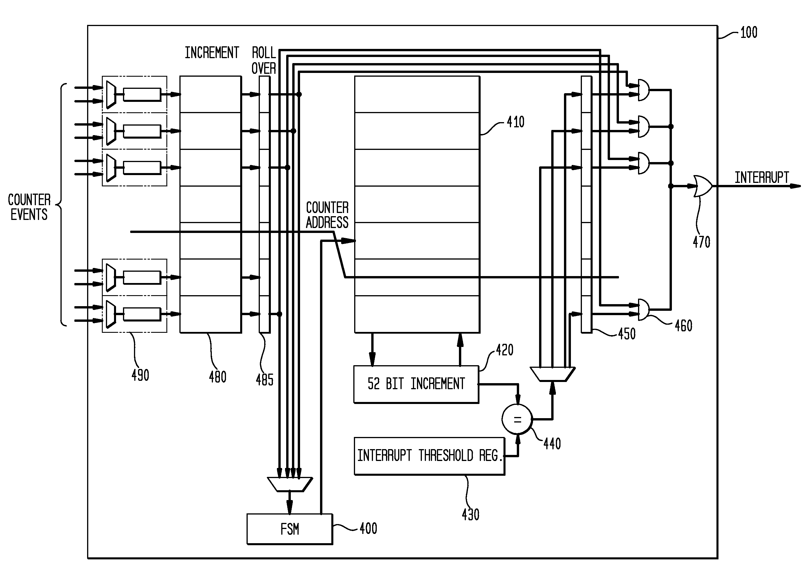
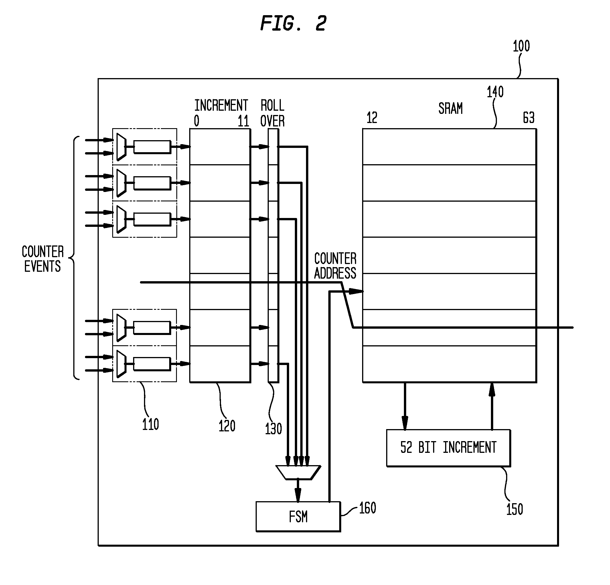
[0060]Referring now to drawings, and more particularly to FIG. 2, there is depicted a preferred embodiment of the invention. The performance counter unit 100 contains N of counters. The N counter events to monitor are selected from set of M events selected by the set of N multiplexers 110. The selected performance events are counted in the counter block 120, which implements N counters which are n width representing n least significant bits of a counter. The counters in the block 120 are implemented using discrete registers. In the preferred embodiment, the block 120 implements only lowest 12 bits of 64-bit counters, but it would be obvious to skilled artisans that any number of lower bits can be counted in the discrete register logic block.

[0061]When a counter from the counter block 120 reaches its maximum, its value rolls over to zero, and the corresponding bit in the “roll over bit” block 130 is set, and the counter continues to track performance events.

[0062]The K−n most signifi...


PUM


Abstract

A method and apparatus for transferring wide data (e.g., n bits) from a narrow bus (m bits, where m<n) for updating a wide data storage array. The apparatus includes: a staging latch accommodating m bits, e.g., 32 bits; control circuitry for depositing the m bits of data from a data bus port into the staging latch addressed using a specific register address; and control circuitry adapted to merging the m bit data contained in the staging latch with m bit data from a data bus port, to generate the n bit wide data, for example, 64 bits, that is written atomically to a storage array specified by an address corresponding to a storage array location. Thus, writing a first set of bits to the staging latch is performed by providing, as a target address of a write (store) operation, the mapped address of the staging latch, and then providing a subsequent set of bits (the remaining bits) together with an array element target specification (encoded as a plurality of the bits of the address specified in the write transaction), in a subsequent write transaction (store).

Description

CROSS-REFERENCE TO RELATED APPLICATIONS[0001]The present application relates to commonly-owned, co-pending U.S. patent applications Ser. No. ______ [Docket No. 19829; YOR920060335US1]; Ser. No. ______ [Docket No. 19830; YOR9200600336US1] and, Ser. No. ______ [Docket No. 19832; YOR920060338US1], each of which was filed on even date herewith.BACKGROUND OF THE INVENTION[0002]1. Field of the Invention[0003]The present invention generally relates to computer systems using single or multiprocessor architectures and, more particularly, to a novel implementation for communicating data from a bus to a wide data storage array, wherein the bus is of a narrow data width as compared to the data width of the array to which data is to be transferred.[0004]2. Description of the Prior Art[0005]Many processor architectures include on a chip a set of counters that allow counting a series of processor events and system events on the chip, such as cache misses, pipeline stalls and floating point operati...

Claims


Application Information

Patent Timeline
Patent Type & Authority Applications(United States)
IPC IPC(8): G06F13/38
CPCG06F13/4018Y02B60/1235Y02B60/1228Y02D10/00
Inventor GARA, ALAN G.GSCHWIND, MICHAEL K.SALAPURA, VALENTINA
Owner IBM CORP
Why Eureka
Try Eureka