Liquid crystal device, active matrix substrate, and electronic apparatus
- Summary
- Abstract
- Description
- Claims
- Application Information
AI Technical Summary
Benefits of technology
Problems solved by technology
Method used
Image

Examples
first embodiment
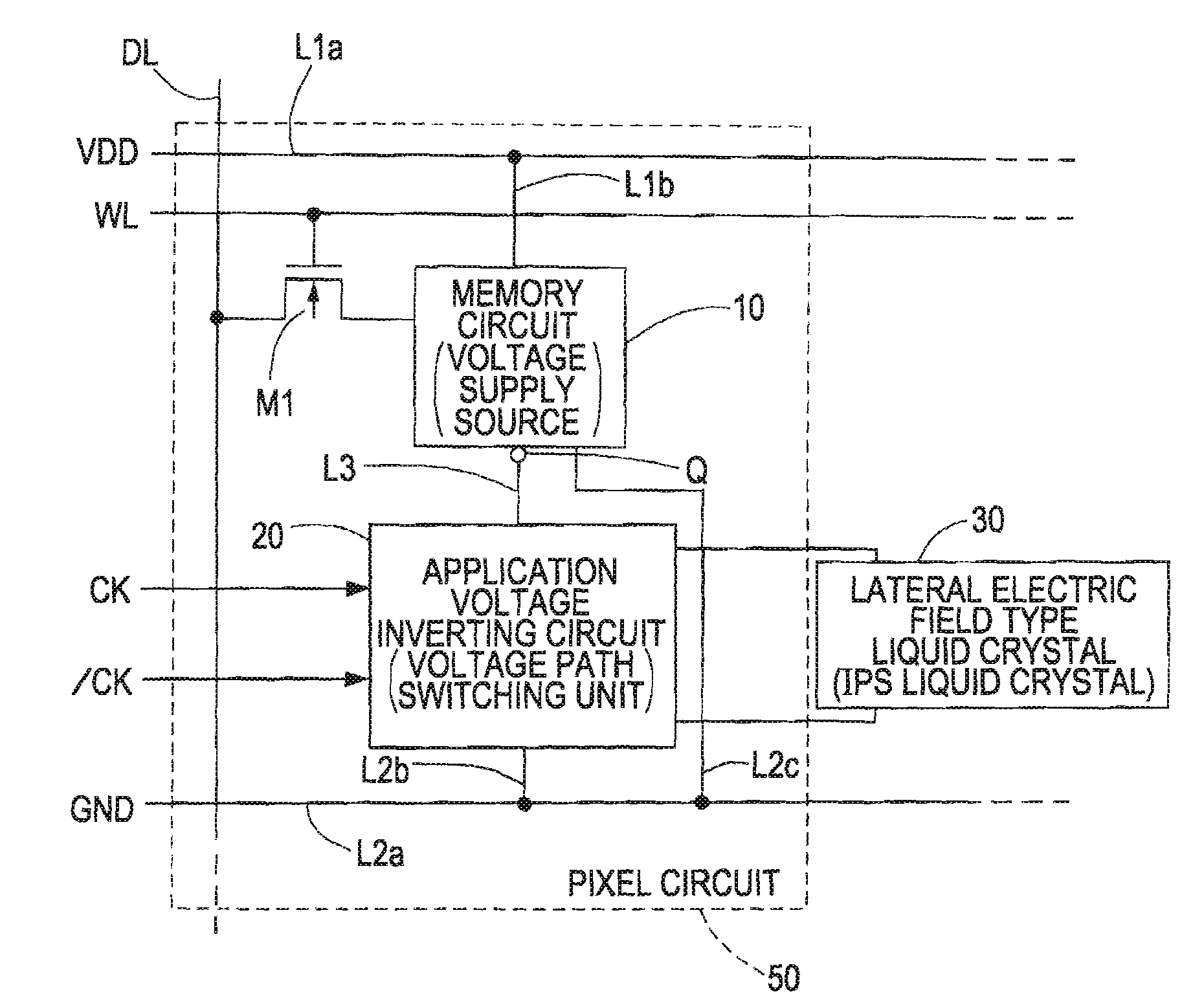
[0069]First, a basic structure of one pixel will be described.
Basic Structure of One Pixel
[0070]FIG. 1 shows a structure of one pixel in a liquid crystal device according to one embodiment of the invention. As shown in FIG. 1, one pixel includes a pixel circuit 50 and a lateral electric field system liquid crystal (herein, called IPS liquid crystal but not limited thereto) 30.
[0071]The lateral electric field system liquid crystal is a liquid crystal having a system in which alignment control of liquid crystal molecules is achieved by applying an electric field parallel to a substrate surface to a liquid crystal layer. This system is called In-Plane Switching (IPS) system or Fringe-Field Switching (FFS) system according to the shape of electrodes by which an electric field is applied to a liquid crystal. The lateral electric field system liquid crystal has a structure in which two electrodes corresponding to one pixel are provided on either one of two substrates having liquid crystal...
second embodiment
[0125]With respect to a second embodiment, a circuit structure which suppresses a penetrating current in an application voltage inverting circuit 20 will be explained.
[0126]FIGS. 9A to 9C are views for explaining a circuit structure and the operation of the application voltage inverting circuit having means suppressing a penetrating current Ipeak. FIG. 9A is a circuit diagram illustrating a circuit structure of the application voltage inverting circuit, FIG. 9B is a timing diagram illustrating the operation of the application voltage inverting circuit, and FIG. 9C is a timing diagram illustrating the operation of a comparative circuit of the application voltage inverting circuit without the means suppressing the penetrating current. In FIGS. 9A to 9C, like elements are referenced by like references.
[0127]The application voltage inverting circuit 20 shown in FIG. 3 has a structure including two pairs of two MOS transistors M7 and M8, M9 and M10 each pair connected in series between t...
third embodiment
[0132]Next, an electronic apparatus, on which the liquid crystal device according to the first embodiment (the reflective type liquid crystal device having SRAMs and using the lateral electric field system liquid crystal) is mounted, will be explained below.
Portable Terminal Having a Sub-Panel
[0133]FIG. 10 is a perspective view illustrating a portable terminal (cellular phone, personal digital assistant (PDA), mobile personal computer, or the like). The portable terminal 1300 shown in FIG. 10 is a cellular phone. As shown in FIG. 10, the cellular phone 1300 includes an upper casing 1304, a sub-panel 100 disposed under the upper casing 1304, a lower casing 1306, and a manipulation key 1302. Further, a main panel is provided on the outer surface of the lower casing 1306 but the main panel is not shown in FIG. 10.
[0134]The sub-panel 100 has a structure including the liquid crystal device according to the first embodiment (the reflective type liquid crystal device with SRAMs, using the ...
PUM
 Abstract
Description
Claims
Application Information