Supercharge Your Innovation With Domain-Expert AI Agents!

Sensor node and circuit board arrangement

a technology of circuit board and node, applied in the field of electronic circuits, can solve the problems of greatly restricted us

Inactive Publication Date: 2008-06-05
HITACHI LTD
View PDF23 Cites 15 Cited by
  • Summary
  • Abstract
  • Description
  • Claims
  • Application Information

AI Technical Summary

Benefits of technology

This configuration improves reception sensitivity, extends battery life, and maintains practical communication distances while reducing battery capacity deterioration, enabling long-term operation with minimal power consumption.

Problems solved by technology

In general, to perform radio communication, a specific transmitter / receiver device preliminarily licensed or authorized must be used, so that use is greatly restricted.

Method used


Image

  • Sensor node and circuit board arrangement
  • Sensor node and circuit board arrangement
  • Sensor node and circuit board arrangement

Examples


Embodiment Construction

[0045]Embodiments of the present invention will be described hereinafter with reference to the drawings. Note that components denoted by the same reference numeral indicate the same or similar configuration.

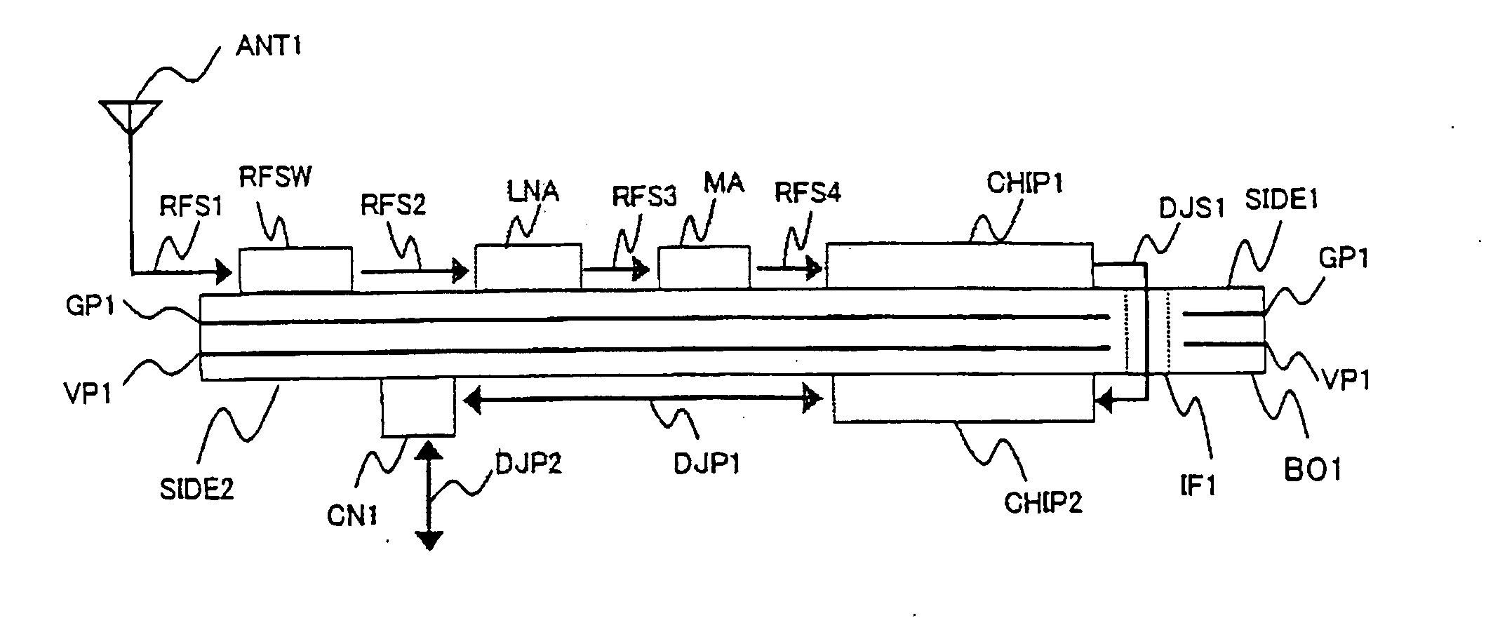
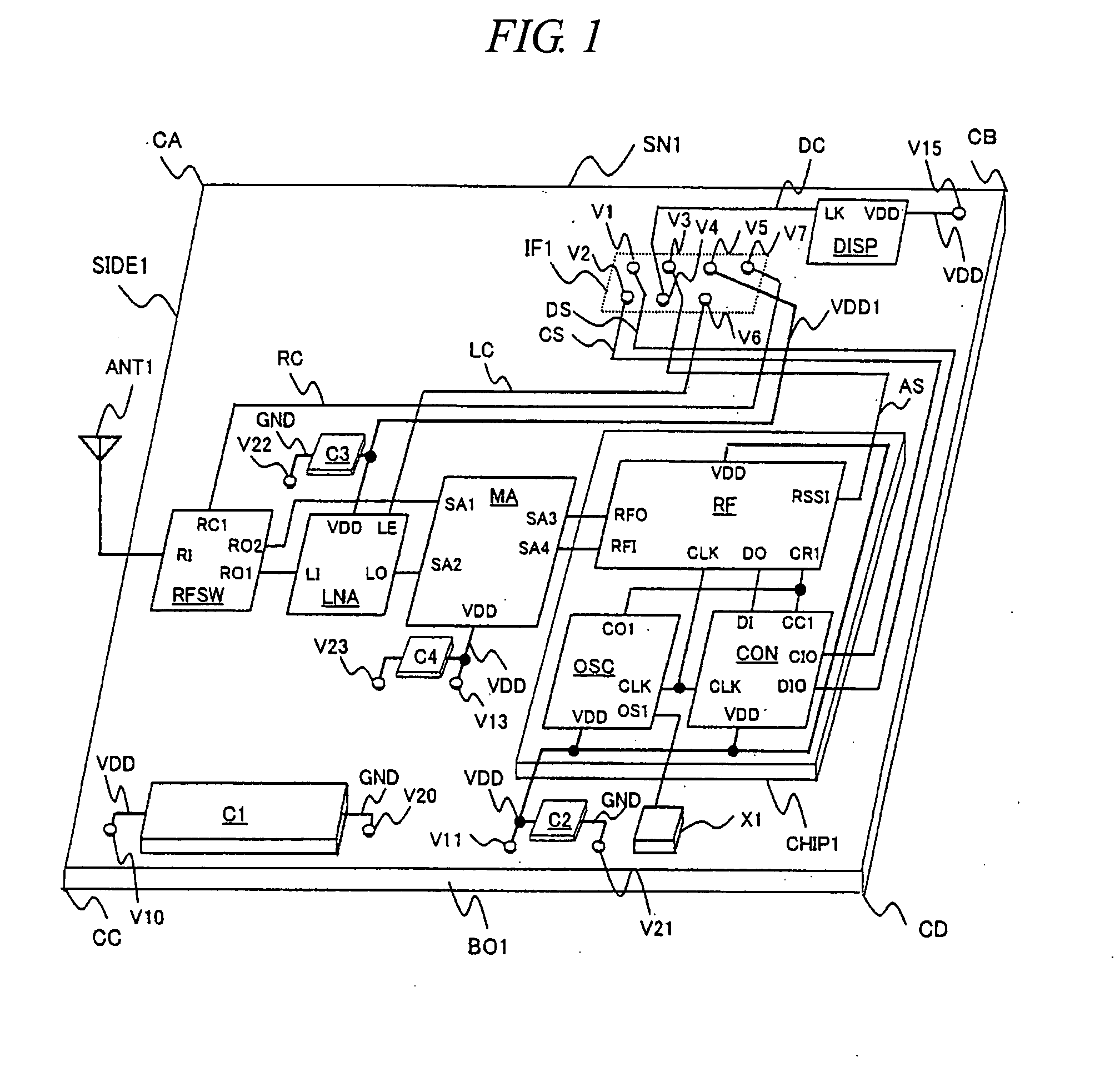
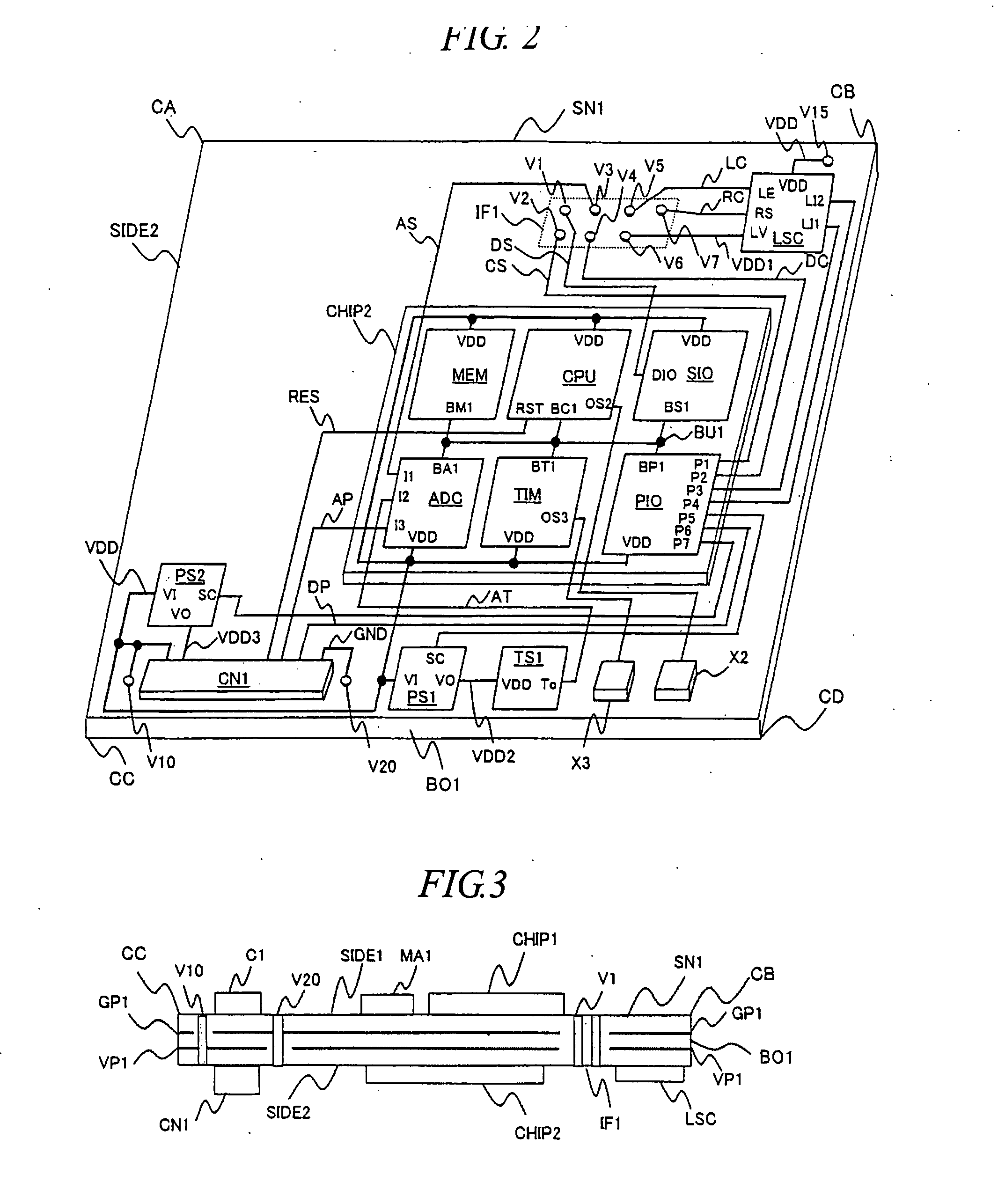
[0046]FIG. 1 shows a state where circuits constituting a sensor node SN1 are mounted on a front side (surface) SIDE1 of a board BO1; and FIG. 2 shows a state where the circuits constituting the sensor node SN1 are mounted on a rear side (surface) SIDE2. Referring to FIG. 1, mounted on the front side SIDE1 of the board BO1 are a high-frequency signal processor chip CHIP1 (hereinafter abbreviated as “RF chip”); a first crystal oscillator X1; a high-frequency switch RFSW; a high-frequency low-noise amplifier LNA; a matching circuit MA; an interface IF1 with the circuits mounted on the rear side SIDE2; a display device DISP; and capacitors C1, C2, C3, and C4. Also, with reference to FIG. 2, the rear side SIDE2 is configured of a processor chip CHIP2; a connector CN1; first and second...


PUM


Abstract

An electronic circuit, preferable as a sensor node, has a highly sensitive radio function and is capable of performing a low-power-consumption operation. The electronic device has a board; a connector for connecting a sensor; a first signal processor circuit receiving an input of sensor data from the sensor through the connector and forming transmission data; and a second signal processor circuit converting a transmission signal from the first signal processor circuit into a high-frequency signal. The connector and the first signal processor circuit are mounted on a first surface of the board, and the second signal processor circuit is mounted on a second surface of the board.

Description

CROSS-REFERENCE TO RELATED APPLICATION[0001]The present application claims priority from U.S. application Ser. No. 10 / 933,270 filed Sep. 3, 2004, which claims the priority of Japanese Patent Application No. 2004-064973 filed Mar. 9, 2004, all of which is incorporated by reference into this application.BACKGROUND OF THE INVENTION[0002]The present invention relates to an electronic circuit equipped with a radio communication function. More specifically, the invention relates to a small and low-power-consumption electronic circuit effectively applied to construct a sensor network system.[0003]In recent years, there has been considered a network system (hereinafter abbreviated as “sensor net”) for capturing in real time various real-world information into an information-processing device by adding, to a sensor, a small electronic circuit having a radio communication function. For the sensor net, widespread application is considered. For example, there is also considered the application ...

Claims


Application Information

Patent Timeline
Patent Type & Authority Applications(United States)
IPC IPC(8): H05K7/00F24F11/02H04B1/38H04B1/44H05K1/00H05K1/02H05K1/18H05K7/06
CPCH05K1/0218H05K1/0298H05K1/181H05K2203/1572H05K2201/10151H05K2201/10689H05K2201/0723Y02P70/50
Inventor YAMASHITA, SHUNZO
Owner HITACHI LTD
Features
  • R&D
  • Intellectual Property
  • Life Sciences
  • Materials
  • Tech Scout
  • Unparalleled Data Quality
  • Higher Quality Content
  • 60% Fewer Hallucinations
Learn More